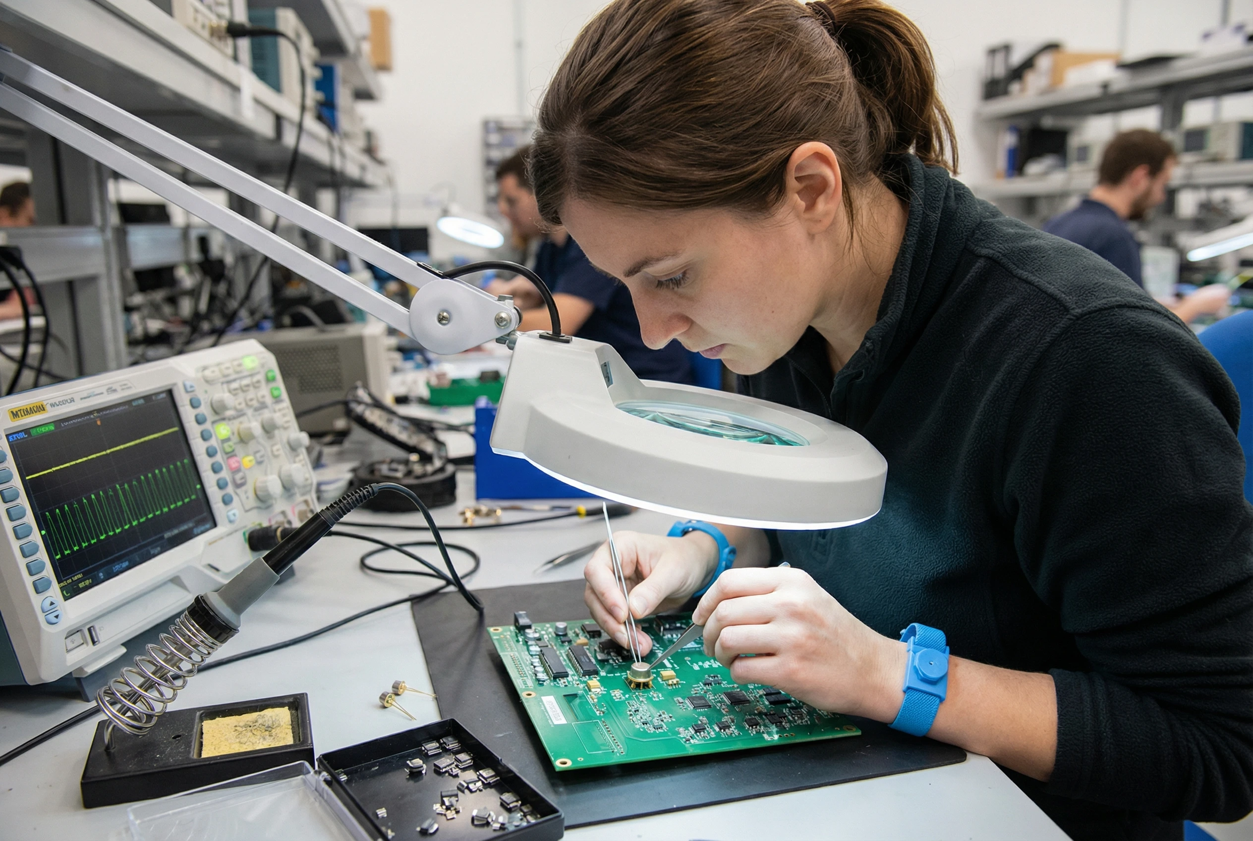
I’ve sat in on way too many design reviews where a brilliant R&D team is pulling their hair out because their prototype is failing. The laser is fine. The readout electronics are perfectly tuned. But the whole system is bottlenecked by a $5 catalog photodiode that just doesn’t fit the physical footprint or lacks the specific spectral response they need.
When you are building next-generation medical diagnostics, LiDAR systems, or specialized analytical instruments, commercial off-the-shelf (COTS) parts usually hit a wall. You end up compromising your entire system architecture just to accomodate a standard sensor. That’s backwards.
If you’re reading this, you probably already know that you need a custom photodetector design. You need a specific active area, a weird package shape, or a custom anti-reflective coating that digi-key just doesn’t sell.
I’m going to walk you through exactly what it takes to go from a napkin sketch to mass production without wasting months of fab time.
Why Off-The-Shelf Ruins Good Engineering
Standard sensors are built for the lowest common denominator. They are designed to be “good enough” for 80% of applications. But if you are in the 20% pushing the boundaries of physics, “good enough” means your product fails.
A custom photodiode design usually starts because of three major pain points:
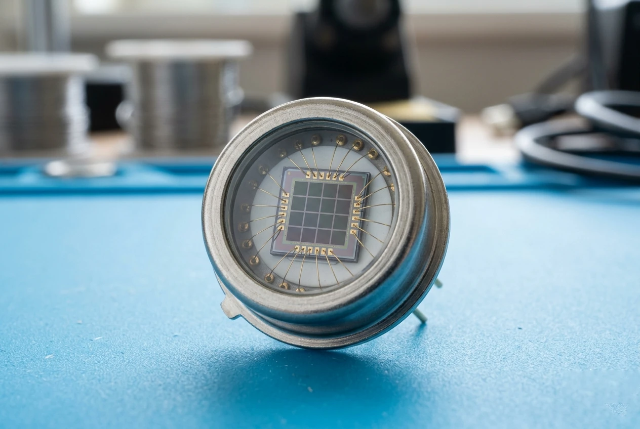
- Geometry constraints: You don’t want a 1x1mm square. You need an annular ring, a 16-element linear array with a pitch of exactly 45 microns, or a quadrant detector with a very specific gap size.
- Parasitic capacitance: Standard TO-cans have lead lengths and package capacitances that kill your high-frequency signals.
- Spectral mismatch: You need peak responsivity at exactly 905nm for your LiDAR, but standard silicon drops off rapidly right where you need it most.
When you transition to a custom photodetector design, you stop fighting the component and start making the component work for your system.
A Controversial Take: Stop Over-Specifying Your Bandwidth!
Alright, here is a hill I will absolutely die on. Most optical engineers ask for way too much bandwidth.
I see RFQs come across my desk all the time asking for an avalanche photodiode or a PIN diode with a 2 GHz bandwidth when their actual pulse duration is 50 nanoseconds.
Why is this a problem? Because in the world of ODM optical components, bandwidth and noise are bitter enemies. If you tell a foundry to give you maximum speed, they are going to thin out the intrinsic layer of the silicon to reduce the transit time of the carriers.
But what happens when you thin the depletion region? Your capacitance skyrockets. And your quantum efficiency at longer wavelengths (like near-infrared) completely crashes because the photons just pass right through the thin silicon without being absorbed.
Unless you are building fiber optic telecom receivers, back off the speed specs. Give your custom photodetector design some breathing room. A thicker depletion region gives you better absorption, lower capacitance, and ultimately a much cleaner signal-to-noise ratio.

Si-PIN-Photodiode mit erhöhter UV-Empfindlichkeit (190-1100nm) PDCT25-F01
Unsere Si-PIN-Diode mit großem Dynamikbereich gewährleistet eine präzise Messung unterschiedlicher Lichtintensitäten. Sie ist ideal für Leistungsmessgeräte und bietet eine hervorragende Linearität über das Spektrum von 190-1100 nm. Eine zuverlässige Si-PIN-Diode für konstante Leistung.
The Physics First: Specs You Actually Care About
When we sit down to engineer a custom photodetector design at BeePhoton, we don’t start with the packaging. We start with the semiconductor physics.
Since you’ll be pasting this right into your notes or editor, I’ll keep the math in plain text so it doesn’t break your formatting.
Reaktionsfähigkeit (R)
This is your basic conversion efficiency. How many amps do you get per watt of optical power?
Formula: R = (I_p) / (P_opt)
Where I_p is photocurrent in Amps, and P_opt is incident optical power in Watts.
If your COTS part gives you 0.4 A/W at 850nm, we can usually push a custom photodiode design closer to the theoretical limit (around 0.6 A/W) by tweaking the anti-reflective (AR) coating thickness specifically for that single wavelength.
Dunkler Strom (I_d)
This is the current that flows when the sensor is completely blindfolded. It’s the enemy of low-light detection. Dark current comes from two places: bulk leakage (defects in the silicon itself) and surface leakage.
In a custom build, we can add physical guard rings around the active area to sink surface leakage away from your transimpedance amplifier (TIA). Standard cheap parts rarely bother with proper guard rings.
Rauschäquivalente Leistung (NEP)
This is the absolute floor of your detection limit.
Formula: NEP = (I_total_noise) / (R)
Your total noise is dominated by shot noise from the dark current.
Shot noise formula: I_shot = square_root( 2 * q * I_d * Bandwidth )
(Where q is the charge of an electron, 1.6e-19 Coulombs).
Notice how Bandwidth is right there in the noise equation? This is exactly why I told you to stop over-specifying it earlier.
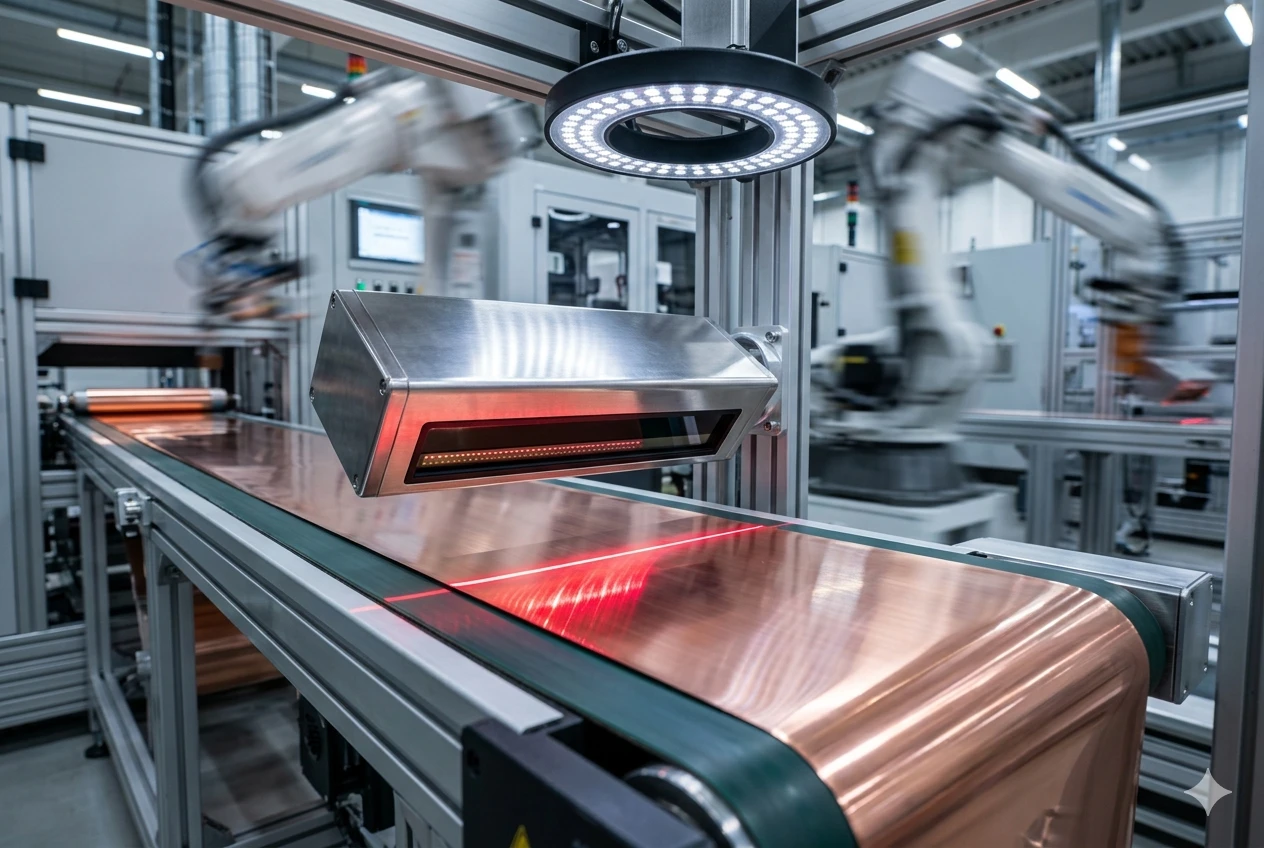
The Workflow: Custom Photodiode Design from Scratch
So, how do we actually get this done? It’s not magic, but it does take a tight process. Moving from prototype to mass production involves a few critical stages.
Stage 1: The Wafer Run (Prototype)
You don’t just order 10 pieces of a custom chip. Semiconductors are built on wafers. Depending on the size of your active area, a single 6-inch or 8-inch silicon wafer might yield anywhere from 5,000 to 50,000 individual chips (die).
During the prototyping phase of a custom photodetector design, we use multi-project wafers or small batch runs. We define the epitaxy (the crystal layers). For instance, if you look at our Si-PIN-Fotodioden, the secret sauce is the “I” (Intrinsic) layer. We can literally grow that layer thicker or thinner depending on whether you prioritize near-infrared absorption or faster rise times.
Stage 2: Masking and Photolithography
You give us a CAD file of the geometry you want. Want a cross-hair shape? No problem. We create a custom photomask. This mask acts like a stencil to block or allow UV light during the etching and doping process. This is where your custom geometry becomes physical reality.
Stage 3: Packaging as OEM Photosensors
A naked piece of silicon (bare die) is useless to most R&D labs unless you have your own wire-bonding machines. This is where ODM optical components really shine.
We take that custom die and put it in a package that fits your mechanical housing.
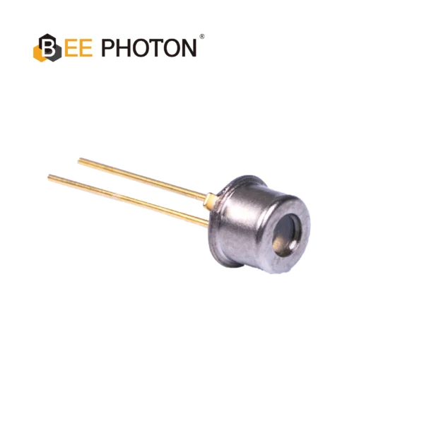
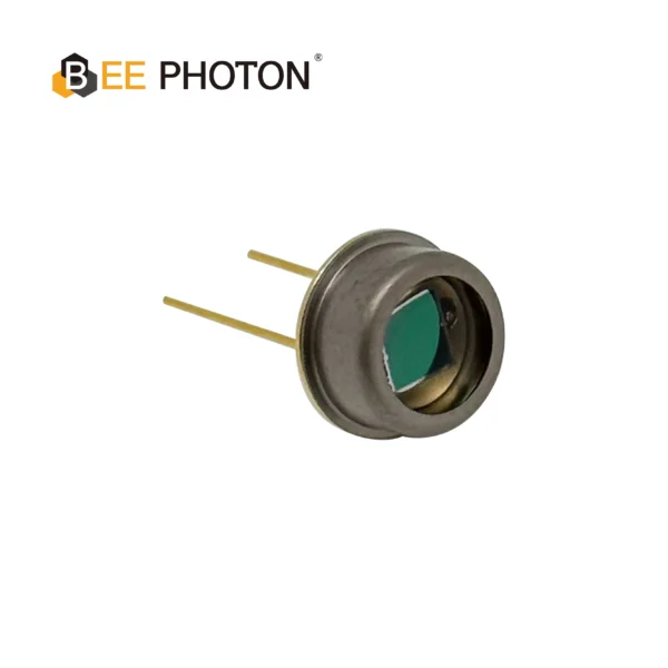
- TO-Cans: Hermetically sealed, great for harsh environments. We can weld a custom window on it (Sapphire, Quartz, or Borosilicate) depending on your UV or IR needs.
- Surface Mount (SMD): Perfect for high-volume automated PCB assembly.
- Ceramic Carriers: Excellent thermal stability if you are cooling the detector with a TEC (Thermoelectric Cooler).
Si-PIN-Photodiode mit niedrigem Dunkelstrom (350-1060nm) PDCT01-201
Erleben Sie überragende Signalklarheit mit unserer Si-PIN-Photodiode, die für extrem niedrigen Dunkelstrom und hohe Stabilität entwickelt wurde. Diese Fotodiode gewährleistet eine präzise Lasererkennung und optische Messungen. Unsere Si-PIN-Photodiode mit niedrigem Dunkelstrom bietet außergewöhnliche Leistung.
Real Numbers: Standard vs. Custom
To give you an idea of why teams go through the trouble of a custom photodetector design, let’s look at a typical comparison for a 5mm² active area sensor used in low-light spectroscopy.
| Spezifikation | Standard Catalog PIN Diode | Custom BeePhoton Design | Why it Matters |
|---|---|---|---|
| Dark Current (at -10V) | 500 pA | 50 pA (with Guard Rings) | 10x lower noise floor for weak signals. |
| Kapazität | 40 pF | 15 pF (Thick Epi-layer) | Allows faster TIAs without peaking/instability. |
| AR Coating Peak | Broadband (400-1100nm) | Narrowband matched to 650nm | Bounces fewer photons, increases specific responsivity. |
| Dead Space (Arrays) | 50 µm typical | 15 µm custom mask | Captures more light in multichannel systems. |
As you can see, you aren’t just paying for a different shape. You are paying for a massive upgrade in signal integrity.
Case Study: Scaling Up a Medical Diagnostic Sensor
I want to share a story from a few years ago (keeping the client anonymous to protect their IP, obviously).
An R&D team was building a 4-channel fluorescence flow cytometer. They were using four seperate standard avalanche photodiodes. The physical layout was a nightmare. The optical path required complex beam splitters just to route the light to four bulky TO-8 cans. Assembly alignment took their technicians 45 minutes per unit.
They reached out for a custom photodetector design.
We looked at their optical path and realized we could ditch the beam splitters entirely. We designed a custom 4-element monolithic silicon array on a single piece of silicon. The pitch exactly matched their diffraction grating.
Because we built it on a single die, the temperature drift across all four channels was identical, meaning their calibration software got infinitely simpler.
Das Ergebnis?
They moved from prototype to mass production in 8 months. Their assembly time dropped from 45 minutes to 3 minutes because it was just a single surface-mount component. The custom OEM photosensors actually cost less at volume than buying four seperate off-the-shelf APDs. That’s the power of doing it right.
Navigating the Transition to Mass Production
Making one perfect chip in a lab is easy. Making 100,000 of them with a tight statistical distribution is where the real engineering happens.
When you transition a custom photodiode design to mass production, you have to care about yield. If your specs are so ridiculously tight that only 10% of the wafer meets the criteria, your unit cost is going to be astronomical.
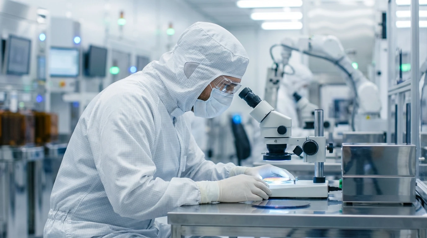
This is why working directly with an experienced fab is critical. We do “wafer-level probing.” Before we even cut the wafer into individual chips, microscopic needles touch down on every single die and measure the dark current and capacitance. We map the entire wafer.
If we notice the edges of the wafer are out of spec, we can adjust the furnace profiles for the next batch. We bin the parts. You only receive the ODM optical components that perfectly match your approved datasheet.
Look, navigating the semiconductor supply chain is notoriously awful right now. You don’t want to be bouncing between a design house in one country, a wafer fab in another, and a packaging facility somewhere else. Things get messy real quick. You lose traceability, and if a batch fails, everyone points fingers at each other. Keep your custom photodetector design under one roof if you can.
Si-PIN-Photodiode mit niedrigem Dunkelstrom (350-1060nm) PDCT14-001
Verbessern Sie Ihre optischen Messgeräte mit unserer Si-PIN-Photodiode im TO-Gehäuse. Sie zeichnet sich durch einen extrem niedrigen Dunkelstrom, hohe Konsistenz und ein Borosilikatfenster für lange Haltbarkeit aus. Diese Hochleistungs-Si-PIN-Photodiode ist für anspruchsvolle Anwendungen optimiert.
FAQ on Custom Photodetector Design
I get bombarded with questions about this process, so let’s clear up a few common ones.
1. What is the typical lead time for a custom photodetector design prototype?
It usually takes about 8 to 12 weeks to get the first physical prototypes in your hands. This includes mask design, wafer fabrication, dicing, and initial packaging. Once the prototype is approved, scaling to mass production takes another 6 to 8 weeks depending on the volume of OEM photosensors you need.
2. Is there a minimum order quantity (MOQ) for custom photodiode design?
For the absolute first proof-of-concept, we run prototype batches where you might receive 50 to 100 packaged units. However, because semiconductor manufacturing happens at the wafer level, the real cost efficiencies kick in when you are projecting a mass production run of at least 1,000 to 5,000 units annually.
3. Can you customize the optical window and filters inside the package?
Absolutely. This is a huge part of custom ODM optical components. We can integrate bandpass filters directly onto the silicon die or swap the standard glass window of a TO-can for materials like Sapphire or UV-fused silica. This eliminates the need for external optical filters in your final device assembly.
Let’s Build Exactly What You Need
If your R&D team is burning engineering hours trying to force a catalog sensor into a cutting-edge system, you are losing money and time to market. You don’t have to compromise your system architecture.
Whether you need ultra-low dark current for a fluorescence detector, a weird physical geometry for an encoder, or you just need a reliable supply chain for mass-produced OEM photosensors, we’ve got the cleanrooms and the engineering scars to make it happen.
Stop wrestling with datasheets that almost work. Shoot us an email if you’re stuck, and let’s talk about the physics of your specific application.
Reach out directly at info@photo-detector.com oder gehen Sie zu unserem Kontakt page to drop us your target specs. We’ll review your requirements and let you know exactly what a custom photodetector design will look like for your project.