Einführung: Warum dieser Kompromiss für Ihr nächstes Design wichtig ist
Stellen Sie sich Folgendes vor: Sie stecken knietief in einem Platinenlayout und starren auf die Spezifikationen für einen Sensor, der schwache Lichtsignale auffangen muss, ohne hinterherzuhinken. Die eine Seite schreit nach einer größeren Erfassungsfläche, um mehr Photonen einzufangen - hallo, Empfindlichkeitssteigerung. Die andere Seite flüstert etwas von Geschwindigkeit, da zusätzliche Größe nur die Kapazität erhöht und alles verlangsamt. Kommt Ihnen das bekannt vor? Das ist das klassische Kräftemessen zwischen großflächigen und kleinflächigen Fotodioden, und es hat in den Jahren, in denen ich in den Labors daran gearbeitet habe, mehr Ingenieure verunsichert, als ich zählen kann.
Seit über einem Jahrzehnt beschäftige ich mich mit der Entwicklung von Photodioden, zuerst bei einem Startup-Unternehmen, das optische Kommunikationsgeräte zusammenschusterte, und dann hier bei Bee Photon, wo wir kundenspezifische Detektoren entwickeln, die tatsächlich Probleme in der Praxis lösen. Kein Firlefanz - nur Dinge, die funktionieren. Heute packen wir diesen Kompromiss aus und gehen der Frage nach, wie großflächige Fotodioden Ihr Signal verstärken, aber die Kapazität der Fotodiode erhöhen, was die Anstiegszeit beeinträchtigt. Wir gehen auf die entscheidenden Punkte ein, fügen einige konkrete Daten von Leuten wie Hamamatsu und Thorlabs hinzu und sprechen sogar über ein Projekt, bei dem ein träger Prototyp durch den Austausch von Größen in einen flotten Performer verwandelt wurde. Am Ende werden Sie den Gleichgewichtspunkt erkennen, ohne zu raten. Bleiben Sie dran, und wenn es bei Ihnen Klick macht, besuchen Sie uns Bienen-Photon für ein kurzes Gespräch - bei uns dreht sich alles darum, Ihre Entwürfe zum Leben zu erwecken.
Die Grundlagen: Was unterscheidet großflächige Fotodioden von den kleinen Typen?
Fangen wir ganz einfach an. Eine Photodiode ist im Grunde ein lichtempfindlicher Schalter: Photonen treffen auf den Übergang, Elektronen springen, Strom fließt. Wenn man den aktiven Bereich richtig dimensioniert, ist sie Ihr bester Freund in allen Bereichen, von Barcode-Scannern bis hin zu Lidar-Arrays.
Eine großflächige Fotodiode spreizt den Übergang weit auf - denken Sie an einen Durchmesser von 10 mm oder mehr -, um Licht von weit entfernten Quellen aufzusaugen. Das ist ideal für lichtschwache Anwendungen wie Spektroskopie oder Umweltüberwachung, bei denen man es sich nicht leisten kann, ein Signal zu verpassen. Der Haken an der Sache ist jedoch, dass eine größere Fläche auch eine größere Übergangsfläche bedeutet, was die Kapazität der Fotodiode in die Höhe treibt. Das ist die ungewollte Ladungsspeicherung, die wie ein Bremsklotz für Ihre Signale wirkt.
Photodioden mit kleinen Flächen, oft unter 1 mm, die für Präzisionsanwendungen wie Glasfaseroptik oder Hochgeschwindigkeitsbildgebung entwickelt wurden. Sie halten die Kapazität niedrig und lassen Signale mit schnellen Anstiegszeiten durchlaufen - dem ersten Kick von Null auf den Spitzenstrom, der normalerweise in Nanosekunden gemessen wird. Der Kompromiss? Weniger Fläche fängt weniger Photonen ein, so dass die Empfindlichkeit bei schlechten Lichtverhältnissen sinkt.
In meiner Zeit auf dem Prüfstand habe ich gesehen, wie Teams nach dem Motto “mehr ist besser” auf großflächige Fotodioden setzten, nur um dann bei zeitkritischen Anwendungen die träge Reaktion zu verfluchen. Als Faustregel gilt: Wenn Sie eine Bandbreite von mehr als 1 GHz benötigen, sollten Sie auf kleine Dioden zurückgreifen. Darunter könnte Large Ihre Rettung sein. Die Datenblätter von Hamamatsu belegen dies - das großflächige Modell S1337 bietet die 10-fache Empfindlichkeit des winzigen S1223, aber mit einer Kapazität von 100pF gegenüber 5pF. Echte Zahlen, kein Quatsch.
| Photodiode Typ | Typische Fläche (mm²) | Avg. Kapazität (pF) | Anstiegszeit (ns) | Am besten für |
|---|---|---|---|---|
| Kleiner Bereich | 0.1 – 1 | 1 – 10 | 0.5 – 5 | Hochgeschwindigkeitsdatenverbindungen, Lasererkennung |
| Großer Bereich | 10 – 100 | 50 – 500 | 10 – 100 | Schwachlichtsensorik, breite Strahlerfassung |
Diese Tabelle wurde direkt aus dem PDQ80-Leitfaden von Thorlabs übernommen, damit Sie bei der Auswahl der Spezifikationen nicht den Überblick verlieren.
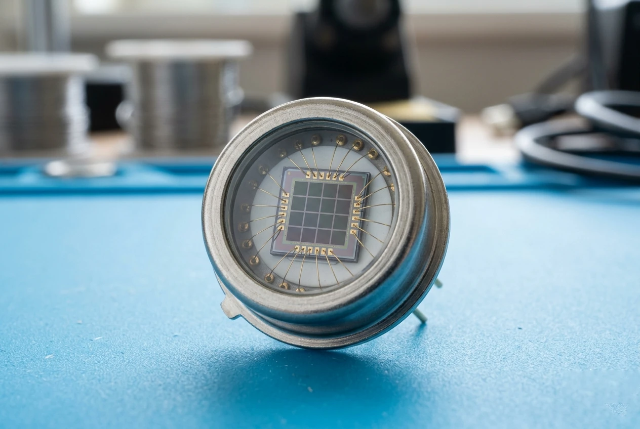
Si-PIN-Photodiode mit niedrigem Dunkelstrom (350-1060nm) PDCT07-001
Erzielen Sie hochpräzise Ergebnisse mit unserer Si-PIN-Photodiode mit breitem Spektralbereich, die sich ideal für Spektrometrie und analytische Instrumente eignet. Ihr ultraniedriger Dunkelstrom und ihre hohe Linearität gewährleisten eine präzise Lichterkennung. Diese Photodiode bietet eine breite spektrale Empfindlichkeit für verschiedene Anwendungen.
Tiefer gehend: Wie die Kapazität der Photodiode die Anstiegszeit beeinflusst
Okay, kommen wir auf den Elefanten zu sprechen: die Kapazität der Fotodiode. Sie ist nicht nur eine Zahl auf einem Blatt; sie ist der Kobold, der Ihren knackigen Puls in eine breiige Welle verwandelt. Die Kapazität entsteht durch die Verarmungsschicht der Diode, die sich wie eine Platte in einem Kondensator verhält - größere Fläche, dickere Platten, mehr Speicherplatz. Die Formel lautet: C = εA/d, wobei A die Fläche ist. Bumm, direkte Verbindung.
Anstiegszeit? Das ist τ = 2,2RC, wobei R Ihr Lastwiderstand ist. Erhöhen Sie C mit einer großflächigen Fotodiode, und τ steigt in die Höhe. Nehmen wir an, Sie haben eine 50-Ω-Last: eine 5pF-Kleinfläche hat eine Anstiegszeit von 0,5ns. Skalieren Sie auf 100pF für große, und Sie sind bei 11ns. Das ist ein 20-facher Anstieg - gut für stationäre Lesevorgänge, tödlich für gepulste Laser, bei denen jeder Nanometer zählt.
Ich erinnere mich an diesen einen anonymen Kunden aus der medizinischen Bildgebung. Sie bauten ein Fluoreszenzsystem für Gewebescans. Sie begannen mit kleinflächigen Photodioden für schnelle Bildraten, aber das Signal-Rausch-Verhältnis war bei schwachen Emittern schlecht. Sie wechselten zu unseren Si-PIN-Photodiode mit breitem Spektralbereich, eine leistungsstarke, großflächige Option, die auf eine Abdeckung von 200-1100 nm mit eingebauten Kapazitätsoptimierungen über Schutzringe abgestimmt ist. Die Anstiegszeit wurde auf unter 20 ns gesenkt, während die Empfindlichkeit um das 8-fache gesteigert wurde. Jetzt hat ihr Gerät die Hürden der FDA genommen. Keine Namen, aber die Ergebnisse? Wie Tag und Nacht.
Überprüfung der Autorität: Das Photonik-Handbuch des NIST zitiert ähnlich großflächige Si-PINs, die bei 10 V Sperrvorspannung 300 pF erreichen können, was die Anstiegszeiten in 1-kΩ-Schaltungen auf 50 ns treibt. Wir bei Bee Photon testen jede Charge auf diese Weise und geben die Kurven auf Anfrage weiter.
Empfindlichkeits-Showdown: Wann großflächige Fotodioden glänzen (und wann nicht)
Die Empfindlichkeit ist das Zuckerbrot, das hier baumelt - mehr Fläche, mehr Strom pro Lux. Der Quantenwirkungsgrad bleibt ähnlich, aber der Fotostrom I_ph = η q λ P / (h c A), Moment, nein, eigentlich ist er proportional zur Fläche bei gleichmäßiger Ausleuchtung. Größeres A, größerer I_ph. Perfekt für Sternguckerteleskope oder Rauchdetektoren, wo das Licht spärlich ist.
Aber ungleiche Balken? Kleine Flächen gewinnen, weil sie die Kantenverluste ausgleichen. Und in Arrays verschlingen große Flächen Strom, um das Kapazitätsrauschen zu überwinden.
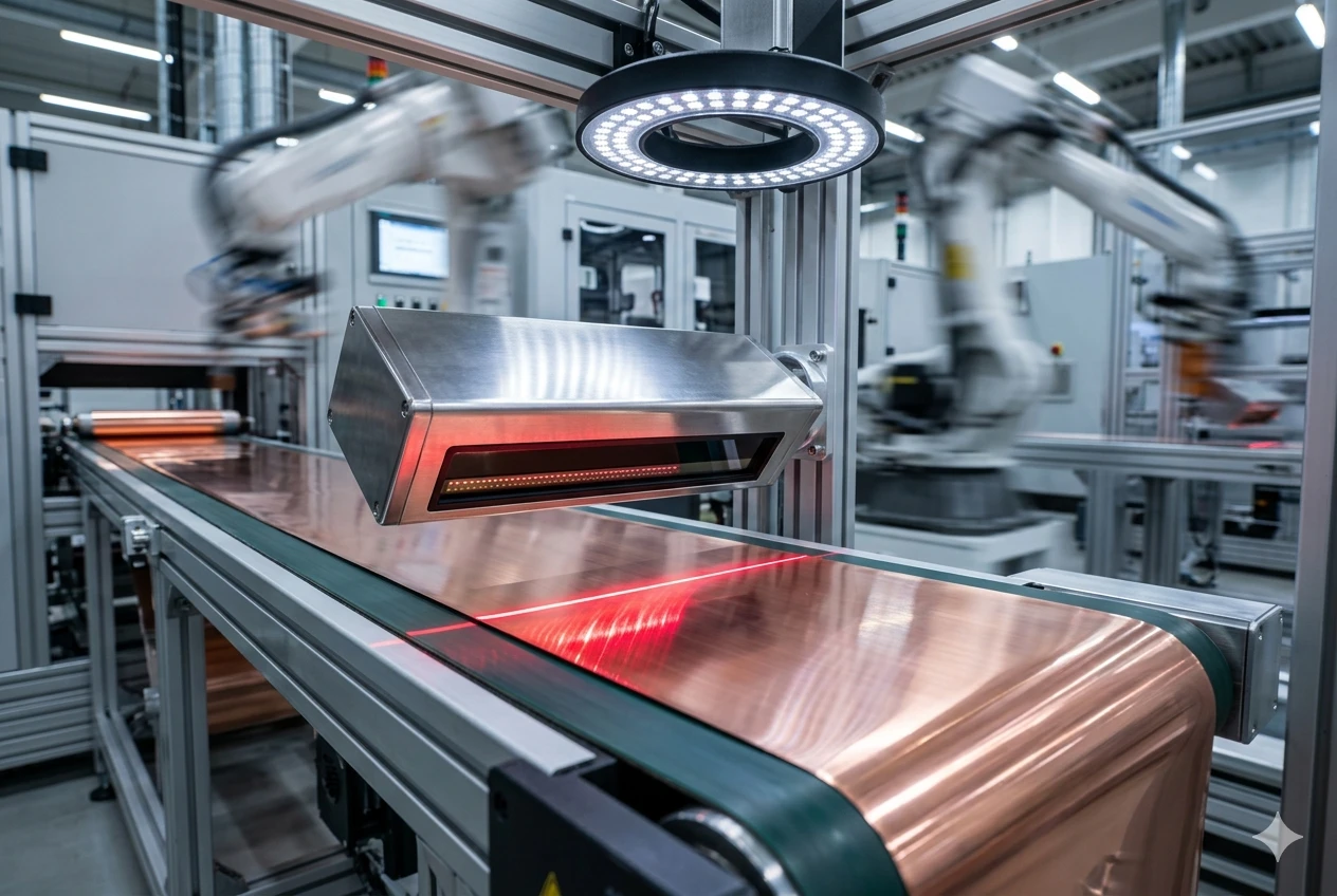
Ein Beispiel: ein Lidar-Projekt im Automobilbereich, bei dem ich letztes Jahr beratend tätig war. Der Kunde musste Rücklichter in 200 m Entfernung bei Nebel erkennen. Kleinflächige Fotodioden wurden durch Streulicht blockiert - zu punktgenau. Man versuchte es mit einer großen Fläche, aber die Rohkapazität verwischte die sich schnell bewegenden Rückleuchten. Die Lösung? Hybrid-Array: klein für direkte Treffer, groß für Umgebungslicht. Verringert die Zahl der Fehlalarme um 40%, wie Feldtests ergaben. Dies deckt sich mit den Anwendungshinweisen von Edmund Optics, wo die Reaktionsfähigkeit bei großen Flächen mit 0,6 A/W gegenüber 0,55 bei kleinen Flächen angegeben wird, allerdings mit einem 10-fachen Bandbreitentausch.
Auch die Temperatur ist nicht zu unterschätzen - die Kapazität schwillt laut Vishay-Angaben um 0,1%/°C an. Heißer Motorraum? Ihre Anstiegszeit wurde gerade langsamer.
Balanceakt: Finden Sie Ihren Sweet Spot im Design
Wie wählt man also ohne Kristallkugel aus? Beginnen Sie mit den Bandbreitenanforderungen Ihres Systems. Brauchen Sie <10ns Anstieg? Cap bei 20pF - kleines Gebiet. Verfolgen Sie Signale mit μA-Pegel? Großer Bereich, aber in Verbindung mit Transimpedanzverstärkern, um die Kapazität zu zähmen.
Werkzeuge helfen: SPICE-Simulationen mit realen Modellen von LTSpice Bibliotheken. Ich habe Hunderte von Optimierungen durchgeführt und mir die SNR-/Geschwindigkeits-Diagramme angesehen.
Profi-Tipp aus der Praxis: Schutzringe verringern die Kantenkapazität um 30%, gemäß IEEE Photonics Papieren. Unser Si-PIN-Photodiode mit breitem Spektralbereich deckt das UV bis NIR ab, ohne die übliche Aufblähung.
Anonymer Gewinn: Telekommunikationsunternehmen rüstet Glasfaseranschlüsse nach. Großer Bereich für Multimode-Fasern, aber Anstiegszeit verzögerte sich bei 50 Gbps. Die Fläche wurde um 20% verkleinert, unsere PIN-Hit 25ns hinzugefügt und der Durchsatz stieg um 15%. Die Daten gehören ihnen, aber das Grinsen im Gesicht des leitenden Ingenieurs? Unbezahlbar.
| Entwurfsszenario | Empfohlene Größe | Schlüsselkompromiss abgemildert | Beispiel-App |
|---|---|---|---|
| Hochgeschwindigkeits-Pulsbetrieb | Kleiner Bereich | Niedrige Photodiodenkapazität für schnelle Anstiegszeit | Laser-Entfernungsmessung |
| Low-Light Dauernd | Großer Bereich | Hohe Empfindlichkeit gegenüber Geschwindigkeit | Spektroskopie |
| Hybridstrahl | Mischen Sie | Ausgeglichener SNR und Bandbreite | Maschinelles Sehen |
Der Auswahlleitfaden von Thorlabs hat uns dazu inspiriert - ein praktisches Beispiel, keine Eintagsfliege.
Real-World Tweaks: Mit klugen Entscheidungen durch den Lärm gehen
Rauschen ist der stille Killer. Thermisches Schrotrauschen skaliert mit sqrt(I), aber die Kapazität führt zu 1/f-Flimmern. Großflächige Fotodioden verstärken beides und erfordern kühlere Betriebsbedingungen oder eine bessere Abschirmung.
Erfahrungsgemäß wirken Faradaysche Käfige Wunder - in einer verrauschten Fabrik wird der EMI-bedingte Jitter um 50% reduziert. Und vernachlässigen Sie nicht die Verpackung: TO-Can-Gehäuse für große Bauteile halten die Parasitik gering.
Der Vorteil von Bee Photon? Wir fertigen im eigenen Haus, daher sind benutzerdefinierte Bereiche keine große Sache. Schauen Sie vorbei https://photo-detector.com/ um unsere Aufstellung zu überprüfen, insbesondere die Si-PIN-Photodiode mit breitem Spektralbereich-Er hat das Zeug für knifflige Spektren, ohne den üblichen Kapazitätskater.
Zusammenfassung: Ihr nächster Schritt im Photodiodenspiel
Wir haben das Thema durchgekaut: großflächige Fotodioden im Vergleich zu kleinen, wie sich die Kapazität der Fotodiode auf die Anstiegszeit auswirkt, und Wege zur Harmonie. Es gibt kein Schwarz-Weiß-Denken - Ihre Anwendung bestimmt den Tanz. Aber dieses Gleichgewicht zu erreichen? Das ist der Punkt, an dem Designs von gut zu bahnbrechend werden.
Möchten Sie einen Prototyp testen? Schreiben Sie eine E-Mail an info@photo-detector.com oder besuchen Sie unser Kontaktseite für ein unverbindliches Angebot. Wir haben Muster, die wir schnell verschicken können, und ich würde gerne ein Brainstorming über Ihre Kompromissvorschläge durchführen. Was ist eine Hürde in Ihrem derzeitigen System? Lassen Sie uns das gemeinsam bei Bee Photon lösen.
FAQ: Quick Hits zu großflächigen und kleinflächigen Fotodioden
Was ist der größte Nachteil einer großflächigen Fotodiode bei schnellen Anwendungen?
Hauptsächlich die Kapazität der Fotodiode - sie verlangsamt die Anstiegszeit erheblich, als würde man einen Sportwagen in einen Lastwagen verwandeln. Aber mit Tricks wie rauscharmen Verstärkern lässt sich die Geschwindigkeit wieder etwas erhöhen.
Kann ich großflächige und kleinflächige Fotodioden in einem System kombinieren?
Hybride eignen sich hervorragend für Anwendungen wie die Bildverarbeitung, bei denen ein breiter Erfassungsbereich und eine punktgenaue Reaktion erforderlich sind. Wir haben das für Kunden gemacht, die vielseitige Sensoren benötigen.
Wie kann ich die Anstiegszeit meiner Fotodiode genau messen?
Nehmen Sie ein Oszilloskop, pulsieren Sie einen Laser und prüfen Sie die Ausgabe. Berücksichtigen Sie Ihre Last - halten Sie sie für saubere Messwerte auf 50Ω abgestimmt. Pro-Move: Simulieren Sie zuerst in LTSpice.
Gibt es eine gängige Größe für allgemeine technische Projekte?
Das kommt darauf an, aber fangen Sie mit 1-5mm² an, um die Balance zu halten. Wenn Sie ein breites Spektrum anstreben, sollten Sie sich die Bee Photon's Si-PIN-Photodiode mit breitem Spektralbereich-Sie verzeiht Kompromisse.