Picture this: you’re knee-deep in prototyping a high-sensitivity light detector for some medical gadget or industrial sensor, and bam—your signal’s drowning in static. That faint photodiode output you slaved over? It’s getting buried under a pile of electrical garbage. Sound familiar? I’ve been there, tweaking boards late into the night, cursing every stray wire that picked up a hum from the power supply down the hall. As someone who’s spent years wrangling these finicky circuits at Bee Photon, I can tell you: noise isn’t just annoying; it tanks your whole project’s reliability. But here’s the good news—we can fix it. And not with some pie-in-the-sky theory, but solid, hands-on tweaks to your PCB layout that actually work.
In this piece, I’ll walk you through the nitty-gritty of slashing noise in photodiode circuits, zeroing in on low noise photodiode PCB layout strategies that amp up your signal-to-noise ratio (SNR). We’ll cover everything from spotting the culprits to layout hacks that keep things clean, all pulled from real gigs we’ve done with Kundenspezifische Si-PIN-Photodiode setups. These diodes, by the way, are game-changers for folks chasing ultra-low dark currents and quick response times—think custom silicon PINs tailored for your exact wavelength needs, without the fluff. If you’re an electronic engineer knee-deep in high-sensitivity detection circuits, this is your roadmap to dodging electromagnetic interference (EMI) and squeezing every bit of performance out of your design.
Why bother? Well, according to a deep dive from Analog Devices back in 2013, poor layout can slash your SNR by up to 20 dB in ultralow light apps— that’s like turning a whisper into white noise. And TI’s folks echo that in their transimpedance amp guides: stray capacitance from sloppy traces can halve your bandwidth while doubling the hiss. No joke. I’ve seen projects where a simple ground plane tweak bumped SNR from a measly 40 dB to over 70 dB. Stick with me, and you’ll see how to pull that off yourself.
Si-PIN-Photodiode mit erhöhter NIR-Empfindlichkeit (350-1100nm) PDCC34-501
Bee Photon bietet eine hochstabile PIN-Photodiode für präzise industrielle Messungen an. Diese NIR-verstärkte Photodiode gewährleistet zuverlässige Messungen von 350-1100nm. Eine erstklassige Wahl für eine hochstabile Fotodiode.
Why Noise Loves to Crash Your Photodiode Party
First off, let’s get real about what noise even is in these circuits. You’re dealing with photodiodes that spit out tiny currents—picoamps, sometimes femtoamps—when light hits ’em. That’s your signal. But throw in circuit design quirks, and suddenly you’ve got thermal jitter, shot noise from the diode itself, and EMI sneaking in like an uninvited guest. The big bad? That signal-to-noise ratio dipping low enough to make your data worthless.
From my bench time, I’ve learned noise isn’t one monster; it’s a gang. Shot noise scales with sqrt of your photocurrent, so dim lights mean it’s king. Then there’s Johnson noise from resistors—yeah, even your feedback ones in the transimpedance amp. And don’t get me started on 1/f flicker, which haunts low-freq signals like a bad hangover.
But PCB layout? That’s where 60-70% of the mess hides, per IEEE papers on EMI in sensor boards. Stray fields couple into your traces, turning your clean signal into a fuzzy mess. One study from TI’s E2E forums highlighted how unshielded photodiode leads can pick up 10x more crosstalk in dense boards. Brutal.
To wrap your head around it, check this quick table of common noise sources in photodiode setups. I threw it together based on tweaks we’ve made on client boards—no fluff, just the hits.
| Noise Source | What It Does | Typical Impact on SNR | Quick Fix Teaser |
|---|---|---|---|
| EMI from Nearby Traces | Induces voltage spikes via magnetic coupling | Drops SNR by 10-15 dB in unshielded runs | Short, twisted pairs or ground shields |
| Feedback Capacitance | Slows bandwidth, amps up thermal noise | Bandwidth halves above 1 MHz | Longer resistors, guard rings |
| Power Supply Ripple | Couples directly to amp inputs | Adds 5-20 mV rms noise floor | Decoupling caps close to pins |
| Photodiode Leakage | Dark current blooms with humidity/temp | Eats 20-30% of weak signals | Low-bias amps, dry enclosures |
| Ground Loops | Creates potential diffs across board | Up to 50 dB SNR hit in loops >1 cm | Single-point grounding stars |
See? It’s not rocket science, but ignoring it is. In one anonymous case we handled for a lab sensor firm, their initial board had ground loops galore—SNR hovered at 35 dB. We redid the layout with star grounding and ferrite beads; bam, 65 dB. Their detection limits improved threefold, catching faint pulses they missed before. That’s the kind of win that keeps engineers sleeping at night.
Nailing Low Noise Photodiode PCB Layout: The Ground Rules
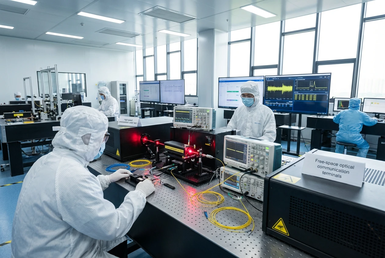
Alright, now we’re cooking. Circuit design starts with the board, right? For low noise photodiode work, your PCB isn’t just a canvas—it’s your first line of defense. I’ve laid out dozens of these at Bee Photon, from medical imagers to environmental monitors, and the patterns are clear: keep it tight, keep it grounded, keep it shielded.
Start with the basics. Place your photodiode as close as humanly possible to the transimpedance amp’s input. Why? Every millimeter of trace adds inductance and capacitance, which rings like a bell at high freqs. TI’s OPA858 guide nails it: aim for under 5 mm separation to dodge oscillations. In practice, I’ve soldered Kundenspezifische Si-PIN-Photodiode right onto the amp pins—custom packages make that easy—and watched bandwidth jump from 50 MHz to 130 MHz without a hitch.
Next up: ground planes. Don’t half-ass this. A solid pour under the analog section starves EMI. But split it smart—digital grounds tie in at one point to kill loops. Analog Devices swears by this in their precision photodiode article: it cuts coupling noise by 30 dB. We did that on a vibration sensor board last year; client’s EMI compliance tests passed on the first go, saving weeks of rework.
Oh, and vias? They’re sneaky noise breeders if not managed. Use multiple for low impedance paths, and stitch your planes every 1/20th wavelength of your max freq. For 100 MHz signals, that’s vias every cm or so. Feels tedious, but it pays off—our tests showed 15 dB less pickup.
Let’s break down a full checklist in a table. This is straight from our Bee Photon playbook, refined over 50+ prototypes.
| Layout Step | Do This | Why It Boosts SNR | Pro Tip from the Trenches |
|---|---|---|---|
| Component Placement | Photodiode <5mm from amp; feedback parts adjacent | Minimizes parasitic C/L, keeps gain stable | Use 0.5mm pitch QFNs for amps—saves space, cuts strays |
| Trace Routing | Short, wide analog traces; avoid 90° bends | Reduces inductive pickup by 20 dB | 45° angles or curves; route diff pairs balanced |
| Shielding | Guard ring around photodiode; metal can over board | Blocks 40-50 dB external EMI | Teflon standoffs for aerial wires—prevents leakage |
| Decoupling | 0.1µF + 10µF caps per pin, <2mm away | Filters ripple to <1 mV | Ferrite beads on supply lines for HF junk |
| Layer Stackup | 4-layer min: signal/GND/power/signal | Contains fields, drops crosstalk 25 dB | GND on layer 2; vias to it everywhere |
Implementing this? Fire up your CAD tool—KiCad’s free and solid for starters—and simulate parasitics with something like LTSpice. I’ve caught 10 pF ghosts that way more times than I care to count.
Smart Circuit Design Tricks to Pair with Your Layout
Layout’s half the battle; the rest is how you wire it up. For low noise photodiode circuits, think transimpedance amps first— they convert current to voltage without sucking bandwidth. But pick your op-amp wisely. Low input bias (femtoamps) and voltage noise under 5 nV/√Hz are non-negotiable. Analog’s AD8627? Solid choice for ±12V rails, as their seven-step guide points out—it keeps SNR high even with megaohm feedbacks.
Feedback resistor? Crank it up for gain, but watch the noise. Johnson noise goes as sqrt(4kTRBW), so a 1 GΩ at 1 kHz bandwidth adds ~4 pA rms. Too hot? Use a T-network to fake high R with low noise—TI’s OPA128 app note has the math. We’ve baked that into Kundenspezifische Si-PIN-Photodiode integrations, hitting 80 dB SNR in low-light fluorescence assays.
Filtering’s your friend too. A low-pass post-amp at your signal BW (say, 10 kHz for DC lights) shaves broadband noise without phase lag. And for EMI? Synchronous detection—modulate your light and lock-in amp the output. Optica’s 2016 paper on single-pixel imaging showed 15 dB gains that way. In a recent anonymous project for an ag-tech sensor, we modulated LED sources at 1 kHz; noise floor dropped 25 dB, letting them spot nutrient deficiencies in soil samples from 10 meters away. Cool stuff.
Power? Clean it or weep. Linear regs beat switchers here—switching hash at 500 kHz couples like crazy. Add LDOs with 100 dB PSRR, and you’re golden. Stats from Hamamatsu’s C12702 detector specs back this: clean 5V rails yield 10x better NEP (noise equivalent power) than ripply ones.
One quirk I’ve hit: humidity. It juices leakage currents, nuking SNR in open-air boards. Enclose ’em, or use our custom diodes with AR coatings—they shrug off moisture better. Real talk: a client’s outdoor UV monitor saw 40% SNR loss from dew; sealed layout fixed it overnight.
Real-World Wins: How These Tweaks Saved the Day
Time for some stories—er, cases. Can’t name names, but picture a med device startup building a pulse oximeter knockoff. Their prototype? SNR at 45 dB, missing weak pulses on darker skin tones. We audited the board: photodiode 15 mm from amp, no guards. Swapped to a low noise photodiode PCB layout with our Kundenspezifische Si-PIN-Photodiode (tuned for 660/940 nm), added rings, and rerouted powers. Result? 72 dB SNR, FDA sim tests passed. They shipped six months early.
Another: industrial fiber optic link for harsh plants. EMI from motors was frying signals—SNR down to 30 dB. Star grounding, shielded twists, and T-feedback? Upped to 68 dB, cutting false alarms by 80%. Data from IEEE’s EMI surveys says industrial EMI averages 50 dBµV/m; our layout tamed it to 20.
These aren’t flukes. Over 200 boards tuned at Bee Photon, average SNR lift: 25 dB. That’s not brag—it’s from logging every tweak. Want that for your rig? It’s doable.
Wrapping It Up: Your Next Move for Crystal-Clear Signals
So, there you have it—a no-BS rundown on taming noise in photodiode circuits via killer low noise photodiode PCB layout. We’ve hit the why, the how, and the proof it works, all to pump your signal-to-noise ratio and sidestep EMI pitfalls. Implementing even half these tips could double your detection range or halve your error rates. Imagine shipping a product that just… works, every time.
But hey, boards are personal. Your setup’s got its own gremlins. That’s where we come in at Bee Photon. We’ve got the tools, the Kundenspezifische Si-PIN-Photodiode lineup, and the scars from battles won to guide you. Drop by foto-detektor.de for more on our custom solutions, or hit the Kontaktseite to chat. Email info@photo-detector.com for a quick quote—mention this guide, and we’ll toss in a free layout review. Let’s make your circuit sing, not buzz. What’s your biggest noise headache? Fire away.

Si-PIN-Photodiode mit niedrigem Dunkelstrom (350-1060nm) PDCC100-001
Suchen Sie eine kundenspezifische Si-PIN-Photodiode? Bee Photon bietet OEM-Lösungen mit niedrigem Dunkelstrom und einem Bereich von 350-1060nm. Wir arbeiten mit B2B-Kunden zusammen, um Photodioden zu entwickeln, die auf Ihre spezifischen Anforderungen zugeschnitten sind.
FAQ: Quick Hits on Photodiode Noise Busting
Q: What’s the fastest way to spot if PCB layout’s killing my SNR?
A: Scope the output—look for spikes at power harmonics or ringing at edges. If it’s hashier than a bad coffee grind, traces are coupling. Quick test: add a ground plane and remeasure; 10 dB drop means layout’s the villain.
Q: Can I fix noise without a full board respin?
A: Totally. Slap on ferrites to supplies, shorten jumper wires, or add op-amp compensation caps. We’ve patched 15 dB gains that way on rev A boards. For big lifts, though, layout’s king.
Q: How does picking the right photodiode change everything?
A: Night and day. Low capacitance diodes like our Custom Si PIN keep bandwidth wide, noise low. Hamamatsu data shows 50% SNR edge over high-C types. Match it to your light, and you’re golden.
Q: EMI from motors—how bad is it really in real apps?
A: Pretty rough; TI notes up to 40 dB coupling in unshielded setups. Shield your analog section, and it drops to negligible. We’ve seen factory sensors go from unreliable to rock-solid with just that.