En el mundo de los semiconductores, “precisión” no es más que una palabra educada para “no estropear la superposición”. Cuando el tamaño de los nodos es invisible para el ojo humano, el margen de error no sólo es escaso, sino que no existe.
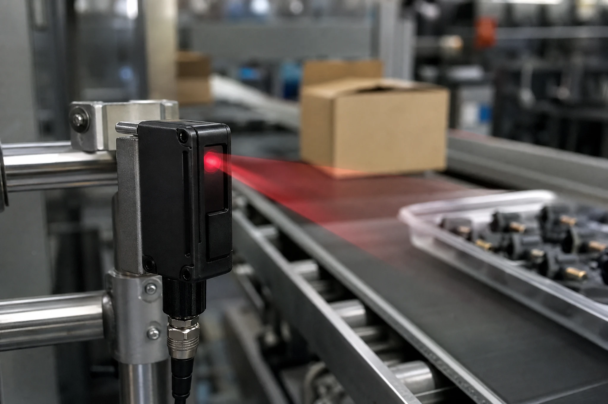
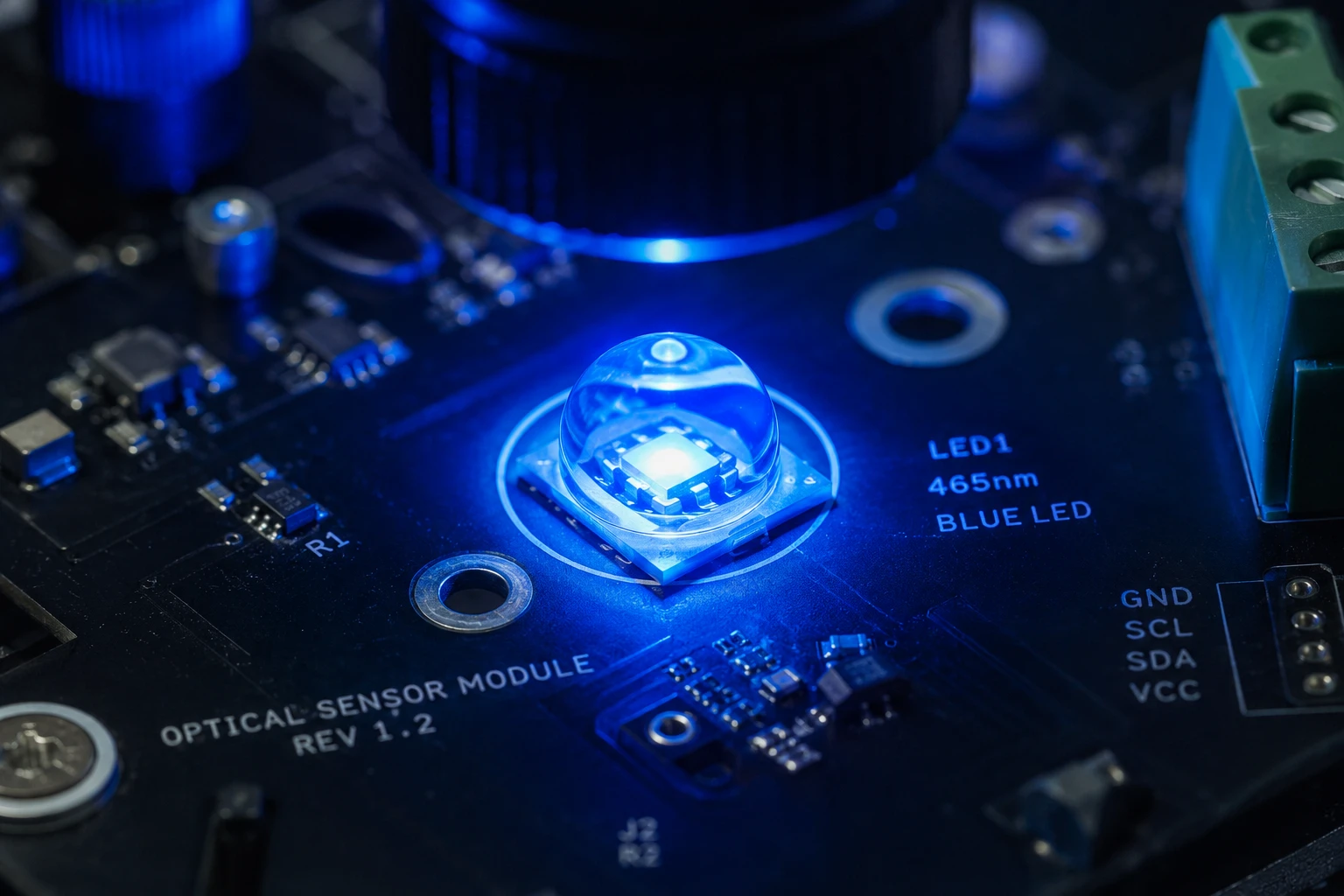
Llevo años indagando en las tripas de las máquinas litográficas, desde los antiguos steppers hasta los nuevos y relucientes escáneres, y he observado un patrón recurrente. Todo el mundo se obsesiona con la fuente láser y la óptica de las lentes. Claro que importan. Pero, ¿con qué frecuencia se revisan los “ojos” de la máquina? Me refiero a los sensores de litografía de semiconductores. En concreto, los fotodetectores UV responsables de la supervisión del haz y la alineación de las obleas.
Si esos sensores se desvían, su rendimiento se reduce. Es así de simple.
Hoy me voy a saltar la palabrería de marketing. Vamos a analizar por qué los sensores estándar fallan en los entornos litográficos de gama alta y a ver cómo se puede mejorar la calidad de la litografía. Fotodetectores UV-como los fotodiodos PIN de Si mejorados- son lo único que se interpone entre usted y un lote de obleas desechadas.
El sucio secreto de los sensores de alineación de obleas
He aquí una opinión controvertida: la mayoría de los problemas de alineación no son mecánicos. Son fallos de retroalimentación óptica.
Tienes un escenario pesado moviéndose a velocidades vertiginosas. Usted depende de sensores de alineación de obleas para indicar al bucle de control dónde se encuentra exactamente esa oblea en relación con la máscara. Hablamos de requisitos de precisión de superposición normalmente inferiores a 2 o 3 nanómetros para nodos avanzados.
¿Cuál es el problema? Los fotodiodos de silicio estándar odian la luz ultravioleta.
En la litografía ultravioleta profunda (DUV) (piense en los láseres ArF de 193 nm), los fotones de alta energía bombardean la superficie del sensor. Con el tiempo, el silicio estándar se degrada. La capacidad de respuesta disminuye. El sensor “se queda ciego”. Cuando el sensor se degrada, la relación señal/ruido (SNR) disminuye y, de repente, sus algoritmos de alineación están adivinando en lugar de midiendo.
Por qué el silicio estándar falla a 193 nm
Recuerdo que hace unos años asesoré a una fábrica de Taiwán. Estaban observando un descenso gradual del rendimiento de sus capas metálicas. La mecánica estaba bien. Los láseres eran estables.
Sacamos los detectores de posición del haz. Eran de silicio estándar. Bajo la radiación de 193 nm, la capa de pasivación de SiO2 de la superficie del chip se había cargado, creando una “capa muerta” que bloqueaba la captación de electrones. Es un fenómeno llamado histéresis o deriva de respuesta.
Si compra sensores de litografía de semiconductores, No basta con mirar las especificaciones del “Día 1” de la hoja de datos. Hay que saber cómo se comporta tras 1.000 horas de bombardeo UV.

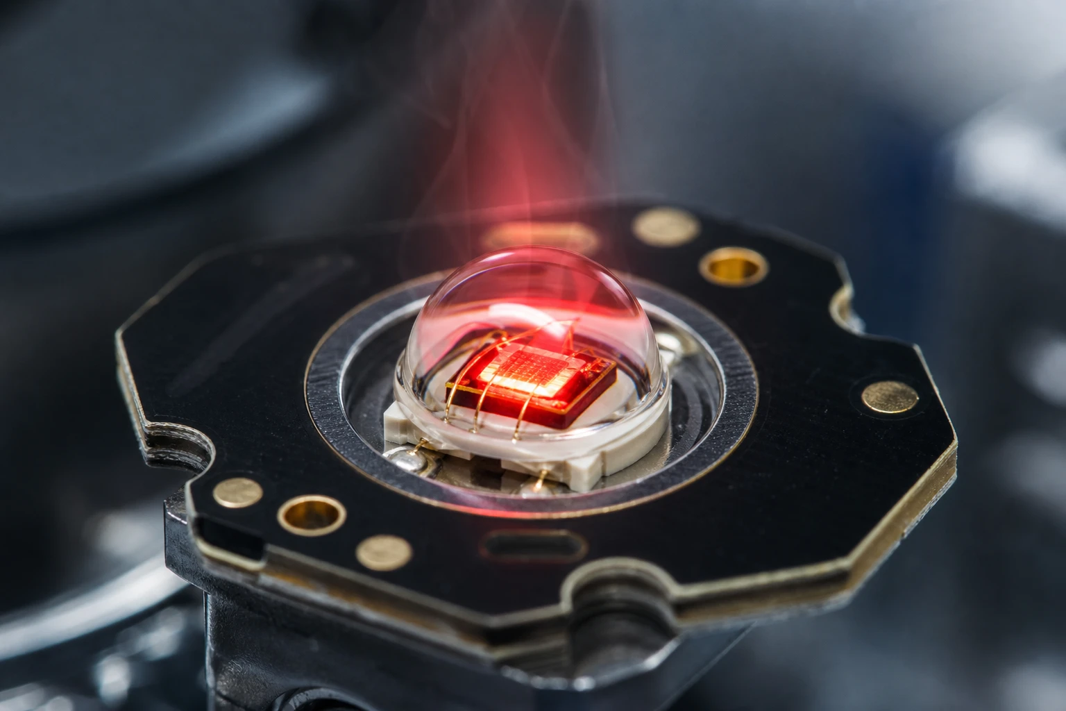
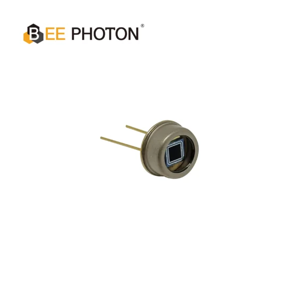
Fotodiodo PIN de Si con sensibilidad UV mejorada (320-1060nm) PDCC100-701
Nuestro fotodiodo PIN de Si de alta respuesta ofrece una señal superior para aplicaciones exigentes. Destaca en la detección de UV con poca luz de 320-1060 nm.
Fotodiodos PIN de Si: La solución de ingeniería
Para solucionarlo, no sólo necesitamos un software mejor, sino una física mejor. Aquí es donde Fotodiodos PIN de Si con sensibilidad UV mejorada entran en juego.
A diferencia de las uniones PN estándar, un diodo PIN tiene una región intrínseca (I) intercalada entre las capas P y N. Esto amplía la región de agotamiento. Esto amplía la región de agotamiento. ¿Qué importancia tiene esto para su equipo litográfico?
- La capacitancia baja: Una menor capacitancia significa tiempos de respuesta más rápidos. Puede escanear más rápido sin retardo de señal.
- Eficiencia cuántica (QE): En las versiones mejoradas con UV, la recombinación superficial se reduce al mínimo. De hecho, se atrapan los fotones UV antes de que sean absorbidos por la capa superficial “muerta”.
En BeePhoton, Lo vemos a menudo. Los ingenieros cambian un sensor genérico por un PIN de Si mejorado con UV especializado y, de repente, sus señales de error de posición (PES) se limpian inmediatamente.
Métricas clave que no puede ignorar
Si está buscando estas piezas, ignore el folleto brillante. Fíjese en estos tres números:
- Respuesta (R) a 193 nm o 248 nm: Medido en A/W (amperios por vatio).
- Resistencia de derivación (Rsh): Esto determina el ruido de fondo. Cuanto más alto, mejor.
- Tiempo de subida (tr): Crucial para escáneres de alto rendimiento.
Aquí tienes un desglose de lo que deberías ver frente a lo que te dan los sensores baratos:
| Característica | Diodo de silicio estándar | Diodo PIN de Si con UV mejorada | Impacto en la litografía |
|---|---|---|---|
| Respuesta UV (193 nm) | < 0,05 A/W | > 0,12 A/W | Señal más potente para la detección de la posición. |
| Estabilidad (Burn-in) | Degrada >10% en 100 h | < 1% degradación | Coherencia de la superposición a largo plazo. |
| Corriente oscura | Alto (rango nA) | Bajo (rango pA) | Mejor contraste en alineaciones con poca luz. |
| Capacitancia de unión | Alta | Bajo | Circuitos de retroalimentación más rápidos para el control del escenario. |
Profundización técnica: La relación señal/ruido (SNR)
Bien, pongámonos técnicos. Prometí fórmulas, y te las voy a dar en texto plano para que puedas usarlas.
Cuando diseñe o sustituya un sensor de alineación de obleas, la batalla se gana o se pierde en la relación señal/ruido. En litografía, la señal óptica reflejada en las marcas de alineación suele ser débil.
La fórmula básica para la SNR en un fotodiodo es:
SNR = I_p / sqrt( 2 * q * (I_p + I_d) * B + (4 * k * T * B / R_sh) )
Vamos a desglosarlo porque parece un lío:
- I_p: Fotocorriente (Señal). Ésta es impulsada por su Responsividad (R) y su Potencia Óptica (P). Entonces, I_p = R * P.
- q: Carga elemental (aprox. 1,6 x 10^-19 C).
- I_d: Corriente oscura. Es el ruido que hace el sensor cuando está muy oscuro. Debe ser BAJA.
- B: Ancho de banda.
- k: Constante de Boltzmann.
- T: Temperatura (Kelvin).
- R_sh: Resistencia de derivación.
Para llevar:
Fíjate en el denominador (la parte inferior). En I_d (corriente oscura) aumenta el ruido. Si tu sensor tiene una corriente oscura alta, tu SNR se reduce.
Además, mire R_sh (Resistencia de derivación). Está en el denominador de una fracción. Esto significa que una Mayor resistencia de derivación da como resultado un término de ruido menor.
Cuando desarrollamos nuestro Fotodiodos PIN de Si con sensibilidad UV mejorada, maximizar esa resistencia de derivación era el objetivo principal. Es la diferencia entre una señal de alineación difusa y un pico agudo.
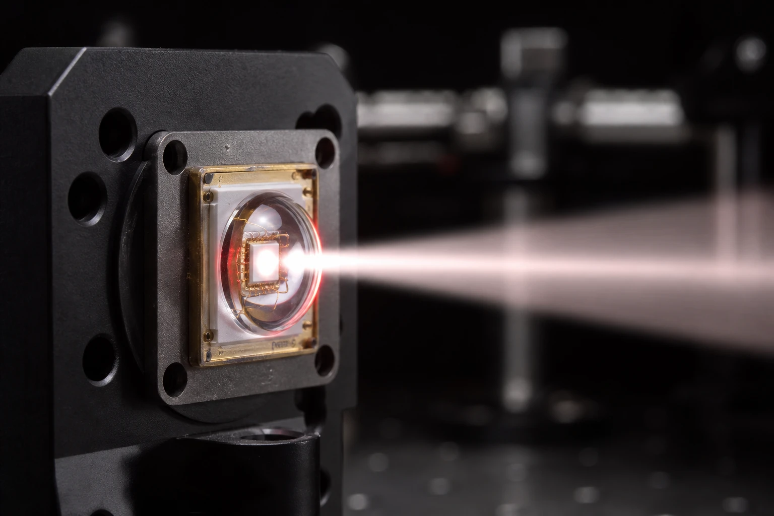
Fotodiodo PIN de Si con sensibilidad UV mejorada (190-1100nm) PDCT06-F01
Consiga una rápida captura de señales con nuestro fotodiodo PIN de Si de tiempo de subida rápido. Optimizado para comunicaciones ópticas y detección de impulsos con baja capacitancia y alta fiabilidad. Consiga hoy mismo el rendimiento de un fotodiodo Si PIN rápido.
Estudio de caso: La crisis de los 7nm
Quiero compartir una historia (nombres eliminados por razones de NDA, obviamente). Una fábrica de tamaño medio especializada en MEMS y algunos chips lógicos heredados estaba tratando de impulsar un escáner adaptado para manejar tolerancias más estrictas.
Se daban contra un muro. La máquina se alineaba, imprimía, y luego la inspección mostraba un error de superposición de 15nm en el eje Y. Al azar.
Culparon a los motores de los escenarios. Culparon al aislamiento de vibraciones. Pasaron semanas recalibrando.
Sugerimos examinar la Fotodetectores UV utilizados en el módulo de prealineación. Resulta que utilizaban sensores antiguos que habían sufrido daños importantes por los rayos UV. Los sensores habían desarrollado una sensibilidad no uniforme en toda la zona activa. Así que, dependiendo de dónde incidiera el láser de alineación en el sensor, la lectura de intensidad variaba ligeramente, lo que engañaba al ordenador haciéndole creer que la oblea estaba centrada cuando no era así.
La solución:
Los cambiamos por PIN de Si de alta estabilidad mejorados con UV.
El resultado:
- El error de superposición del eje Y se ha reducido a < 5 nm.
- Mejora del tiempo de funcionamiento de la máquina (menos necesidad de recalibrado).
- La tasa de chatarra descendió aproximadamente 12% en el primer mes.
Parece una locura que un componente más pequeño que una uña controle el destino de una máquina multimillonaria, pero esa es la realidad del sensores de litografía de semiconductores.
Retos de aprovisionamiento para compradores B2B
Si trabaja en la gestión de compras o ingeniería, sabrá que abastecerse de estas cosas es una pesadilla.
- Obsolescencia: Los grandes fabricantes de sensores suelen abandonar los sensores litográficos de nicho porque el volumen no es el mismo que el de la electrónica de consumo.
- Personalización: Rara vez se necesita una lata TO-5 estándar. Es posible que necesite un soporte cerámico, un material de ventana específico (sílice fundida o zafiro) para soportar los rayos UV, o una forma de área activa personalizada.
- Plazos de entrega: esperar 30 semanas por un sensor es una broma, pero ocurre.
En BeePhoton, intentamos salvar esa distancia. No intentamos venderle un sensor para el mando a distancia de un televisor. Nos centramos en los productos de gama alta. Tanto si necesita un tamaño específico de área activa como una ventana que no solarice bajo luz DUV, lo entendemos.
Puede consultar nuestras especificaciones en el Fotodiodos PIN de Si con sensibilidad UV mejorada página. Merece la pena echarle un vistazo sólo para comparar los gráficos de respuesta espectral con lo que estás utilizando actualmente.
Instalación y manipulación de fotodetectores UV
Aquí hay algo que los manuales rara vez te dicen: las huellas dactilares son fatales.
Cuando se trata de Fotodetectores UV, específicamente para longitudes de onda inferiores a 300 nm, cualquier contaminante orgánico en la ventana (como la grasa de la piel) presentará fluorescencia o absorberá la luz UV.
- Nunca tocar la cara de la ventana. Incluso con guantes.
- Protección ESD: Los diodos PIN de Si son sensibles a la estática. Si se funde la unión durante la instalación, puede que no falle esencialmente. Puede que sólo se vuelva “ruidoso”. En realidad eso es peor porque te pasarás semanas depurando el sistema sin darte cuenta de que el sensor es el culpable.
- Soldadura: Mantenga el calor alejado de la carcasa. El exceso de calor puede desplazar la alineación del troquel dentro del paquete, cambiando el eje óptico.
Tendencias futuras: Más allá de 193 nm
Estamos asistiendo a un cambio hacia detectores aún más complejos para EUV (UV extremo a 13,5 nm). Aunque el silicio tiene dificultades en este campo (a menudo requiere revestimientos especiales o detectores basados en diamante), para la gran mayoría de capas (DUV y UV cercano), el PIN de silicio sigue siendo el rey.
Sin embargo, la demanda de velocidad es cada vez mayor. A medida que aumenta el rendimiento (obleas por hora), el ancho de banda del sensores de alineación de obleas debe aumentar. Estamos llegando al límite de la rapidez de respuesta de un fotodiodo de gran superficie. Es un acto de equilibrio entre el área (más grande es más fácil de alinear) y la capacitancia (más pequeño es más rápido).
Si está diseñando una nueva columna óptica, no deje para el final la elección del sensor. Dicta el diseño de su amplificador, su presupuesto de ruido y, en última instancia, la hoja de especificaciones de su máquina.

Fotodiodo PIN de Si con sensibilidad UV mejorada (190-1100 nm) PDCD100-F01
Experimente una detección UV superior con el fotodiodo sensible al ultravioleta (UV) de Bee Photon.Nuestro fotodiodo PIN de Si garantiza una alta sensibilidad y fiabilidad para instrumentos analíticos.Este fotodiodo sensible al ultravioleta (UV) con ventana de cuarzo ofrece mediciones precisas de 190nm a 1100nm.
Conclusión
La litografía es difícil. Pero tus sensores no deberían dificultarla.
Si observa desviaciones, superposiciones deficientes o caídas inexplicables de la señal, deje de mirar el láser caro y compruebe el fotodiodo barato. Actualizar a una adecuada Fotodetector UV diseñado para el duro entorno de una fábrica es probablemente la medida de mantenimiento con mayor ROI que puede tomar.
No deje que un sensor $50 arruine una oblea $50.000.
PREGUNTAS FRECUENTES: Preguntas frecuentes sobre los sensores litográficos
P1: ¿Por qué no puedo utilizar fotodiodos estándar para aplicaciones de litografía UV?
Sinceramente, se puede, pero no por mucho tiempo. Los fotodiodos de silicio estándar se degradan rápidamente bajo radiación UV de alta energía (concretamente 193 nm y 248 nm). La luz UV daña la pasivación de la superficie, lo que provoca un descenso de la sensibilidad y un aumento de la corriente oscura. Para la litografía, donde la estabilidad lo es todo, se necesita UV mejorada detectores reforzados contra estos daños por radiación.
P2: ¿Con qué frecuencia debemos sustituir los sensores de alineación de obleas?
Depende de la intensidad del láser y del ciclo de trabajo. Sin embargo, una buena regla general es controlar la corriente oscura y la capacidad de respuesta. Si observa una caída de la capacidad de respuesta de más de 5-10% o un aumento significativo del ruido, es el momento. En las fábricas que trabajan 24 horas al día, 7 días a la semana, a menudo vemos ciclos de sustitución preventiva cada 12 o 18 meses en las rutas ópticas críticas para evitar tiempos de inactividad inesperados.
P3: ¿Qué diferencia a los diodos PIN de Si de BeePhoton de los proveedores genéricos?
Nos centramos específicamente en el segmento de alto rendimiento. Nuestra Fotodiodos PIN de Si con sensibilidad UV mejorada cuentan con una alta resistencia a la derivación (para reducir el ruido) y materiales especializados para ventanas que no se oscurecen con la exposición a los rayos UV. Además, entendemos las dificultades de la adquisición B2B: nuestro objetivo es ofrecer mayor disponibilidad y personalización que los grandes distribuidores por catálogo.
¿Está listo para mejorar su precisión?
Si no está seguro de qué sensor se adapta a su columna óptica específica o si necesita un área activa personalizada que se ajuste al perfil de su haz, hablemos.
Hemos ayudado a docenas de fabricantes a estabilizar sus procesos litográficos. No debería tener que adivinar cuando se trata de nanómetros.
- Visite nuestro sitio web: https://photo-detector.com/
- Envíanos un correo electrónico: info@photo-detector.com
- Pida presupuesto: https://photo-detector.com/contact-us/
Póngase en contacto hoy mismo. Asegurémonos de que su próximo lote se alinea a la perfección.