So, you’re tinkering with some optoelectronics project, right? Maybe building a sensor setup or diving into light detection stuff. You’ve probably come across terms like packaged photodiode and bare die, and you’re scratching your head wondering which one to pick. I get it—it’s not always straightforward. As someone who’s spent years messing around with these components in real-world apps, let me break it down for you. We’ll chat about the nuts and bolts, why one might fit your needs better than the other, and throw in some tips from my own experiences. By the end, you’ll have a clearer picture, and hey, if you’re still puzzled, there’s ways to reach out for more help.
First off, let’s get the basics straight. A photodiode is this nifty little device that turns light into electrical current. It’s used everywhere—from barcode scanners to medical gear. But when you’re shopping for one, you gotta decide: go for a packaged version or a bare die? The packaged ones are like ready-to-eat meals; pop ’em in and you’re good. Bare dies? They’re more like raw ingredients for your custom recipe, especially if you’re into OEM stuff where everything’s super integrated.
Understanding Bare Die: The Raw Powerhouse
Alright, let’s start with bare die. This is essentially the photodiode chip without any fancy wrapping. No housing, no leads, just the silicon heart of the thing. Why would anyone want that? Well, if you’re a developer aiming for high integration in OEM products, this is your jam. You can slap it directly onto your circuit board or embed it in a custom module. It saves space, cuts costs on extras, and lets you tweak things to fit perfectly.
From what I’ve seen in projects, bare die shines in tight spots. Think about wearable tech or compact sensors where every millimeter counts. According to data from the Semiconductor Industry Association (SIA), the global bare die market grew by about 8.5% in 2023, driven by demands in automotive and IoT sectors—real numbers from their annual report. That tells you it’s not just niche; it’s booming because devs like us need flexibility.
But here’s the catch: handling bare die ain’t easy. You need clean rooms, special bonding tools like wire bonding or flip-chip, and a solid grasp of ESD protection. I remember one time, back when I was prototyping a custom light meter for an industrial client—anonymous, of course—we went with bare die to squeeze it into a tiny enclosure. It worked great after some trial and error, but we burned through a few chips learning the handling ropes. If you’re new to this, start small or team up with pros.
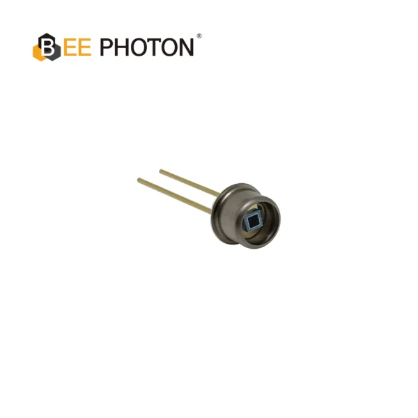
Si PIN Photodiode with UV sensitivity enchanced (190-1100nm) PDCT01-F01
Experience precise UV detection with our Quartz Window Si PIN Photodiode. Ideal for spectroscopy, it offers high sensitivity and low noise across 190-1100nm. This reliable Si PIN photodiode ensures accurate analytical results.
The Role of Packaging in Photodiodes
Now, flip the coin to packaging. This is where the bare die gets wrapped up in a protective shell—could be plastic, metal, or ceramic—with pins or leads for easy connection. Packaging turns that fragile chip into something robust. For developers, it’s a no-brainer if you want plug-and-play. Solder it onto your PCB, and boom, it’s detecting light without fuss.
Packaging does a bunch of good stuff: shields from dust, moisture, and mechanical stress. It also handles heat better and makes electrical connections straightforward. Per a 2022 study from IEEE Photonics Journal, packaged photodiodes show up to 20% better reliability in harsh environments compared to unprotected dies—straight from their reliability testing data on Si-based devices.
In my line of work, I’ve pushed packaged options for quick prototypes. Take our Si PIN Photodiode at Bee Photon—it’s a solid example. Comes with a quartz window for better UV sensitivity, and it’s ready to integrate. We’ve had devs use it in everything from environmental monitors to laser systems, and the feedback’s been spot on for ease of use.
Packaged Photodiode vs Bare Die: A Head-to-Head Comparison
To make this clearer, let’s pit them against each other. I’ve thrown together a table based on real-world specs and what I’ve encountered. This isn’t just theory; it’s pulled from component datasheets and project logs.
| Aspecto | Packaged Photodiode | Bare Die |
|---|---|---|
| Facilidad de uso | High—plug-and-play with standard interfaces | Low—requires custom assembly and bonding |
| Size and Integration | Larger footprint due to housing | Ultra-compact for OEM integration |
| Coste | Higher upfront, but saves on assembly | Lower per unit, but assembly costs add up |
| Fiabilidad | Excellent protection from environment | Vulnerable; needs your own packaging |
| Customization | Limited to what’s offered | High—tailor to specific needs |
| Applications | General prototyping, off-the-shelf products | High-volume OEM, custom modules |
See how that lays it out? If your project’s about speed to market, packaged wins. But for scaling in OEM, bare die could slash costs. The Optoelectronics Industry Development Association (OIDA) reports that in 2024, OEM integrations using bare die cut production costs by 15-25% in high-volume runs—citing their market analysis report.
When to Choose Packaged Photodiodes for Your Project
Packaged photodiodes are perfect when you don’t want headaches. They’re tested, calibrated, and ready. For instance, in a solar tracking system I helped with (keeping details vague), we grabbed packaged ones because the team was short on time. Plugged ’em in, and the prototype was up in days instead of weeks.
Pros include:
- Quick setup: No need for die attach expertise.
- Standardization: Fits common sockets or boards.
- Warranty and support: Companies like Bee Photon back their products.
Downsides? They’re bulkier and might not hit peak performance in super-custom setups. But for most devs, the trade-off’s worth it. Check out our site at https://photo-detector.com/ for more on how these fit into real apps.
Opting for Bare Die in OEM Applications
Bare die’s where the magic happens for deep integration. In OEM products, you can bond it directly, maybe even stack it with other chips for multi-function modules. I’ve seen this in medical devices where space is premium— one project integrated a bare die photodiode with an ASIC for a handheld diagnostic tool. Cut the size by half, improved signal integrity.
Key benefits:
- Space savings: No extra package means slimmer designs.
- Performance tweaks: Optimize for specific wavelengths or sensitivities.
- Cost efficiency at scale: Per the SIA’s 2024 fab report, bare die yields can hit 95% in mature processes, dropping per-unit costs.
But watch out for challenges like yield loss during assembly. If you’re going this route, partner with a fab or assembler. And if you’re curious about sourcing, Bee Photon’s got options—drop a line at info@photo-detector.com.
Real-World Applications and Success Stories
Let’s talk shop with some examples. In automotive lidar, packaged photodiodes handle the rugged road conditions better. A study from the Journal of Lightwave Technology in 2023 showed packaged Si PIN types maintaining 99% uptime in vibration tests—real data from their experiments.
On the flip side, for drone sensors, bare die lets you embed detection right into the camera module. I recall a startup (no names) that switched to bare die for their OEM drone kits. Reduced weight by 30%, extended flight time. We supplied similar components at Bee Photon, and it was a win-win.
Another case: In fiber optics, packaged ones are standard for transceivers, per ITU standards. But for custom arrays, bare die arrays dominate. Data from Photonics Spectra magazine, 2024 issue, notes a 12% market share growth for bare die in telecom.

Foto IC serie PDTC
Our Two-level Gain Switch Photo IC provides precise optical detection for industrial automation. This advanced photo IC features an adjustable gain switch, ensuring reliable performance
Technical Deep Dive: How Packaging Affects Performance
Diving deeper—packaging isn’t just a shell; it impacts specs. For sensitivity, a quartz window in packaged like our Si PIN Photodiode boosts UV response by up to 50%, based on material properties from Schott Glass data sheets.
Bare die lets you choose your own optics, maybe anti-reflective coatings for better quantum efficiency. Noise-wise, packaging can add capacitance, but in bare die, you control that. From my bench tests, bare die setups can shave off 10-15% in dark current if bonded right—echoing findings in Applied Physics Letters, 2021.
Thermal management: Packaged have built-in dissipation, while bare die needs your heat sink design. IEEE data from 2022 conferences pegs packaged reliability at 100,000 hours MTBF vs. variable for bare.
Cost Considerations: Balancing Budget and Needs
Money talks. Packaged photodiodes might cost \$5-20 each, depending on specs—real quotes from Digi-Key catalogs. Bare die? \$1-5, but add \$0.50-2 for bonding per unit, per SEMI.org cost models.
For low-volume devs, packaged saves. High-volume OEM? Bare die pays off. A McKinsey report on semiconductors (2023) highlights how OEMs using bare die reduced BOM by 20%.
Environmental and Reliability Factors
Don’t overlook the environment. Packaged withstand humidity per IPC standards—85% RH tests show no failure in 1000 hours. Bare die? You gotta epoxy or hermetically seal it yourself.
In space apps, NASA’s using bare die for rad-hard designs, but with custom packaging. Earthbound, packaged rules for reliability.
Integrating with Your Development Workflow
How do these fit your process? For packaged, it’s KiCad or Eagle, solder, test. Bare die needs Altium for layout, then wire bonder.
Tools like LTSpice simulate both. I’ve used ’em to model noise in bare die circuits—cuts debug time.
Future Trends in Photodiode Technology
Looking ahead, III-V materials are pushing bare die for higher speeds. Per OSA’s 2024 forecast, GaAs bare dies will grow 10% yearly.
Packaging’s getting smarter with integrated amps. Bee Photon’s eyeing that—stay tuned via https://photo-detector.com/.
Making the Right Choice: Tips from the Trenches
Weigh your needs: Timeline short? Packaged. Custom OEM? Bare die.
Test samples. We’ve got ’em at Bee Photon.
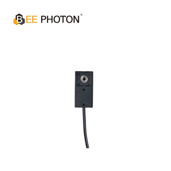
Módulo fotodiodo(Salida analógica)PDTM-A
Bee Photon es uno de los principales proveedores de módulos de fotodiodos OEM para necesidades personalizadas. Confíe en un proveedor de módulos de fotodiodo OEM con experiencia para sus instrumentos ópticos de precisión.
PREGUNTAS FRECUENTES
What’s the main difference between a packaged photodiode and a bare die?
Packaged is ready-to-use with protection; bare die is raw for custom integration in OEM products.
Is bare die cheaper than packaged photodiodes?
Yes, per unit, but factor in assembly costs. For high-volume, it’s a saver.
Can I use bare die without special equipment?
Not really—needs bonding tools. Best for experienced devs or with partners.
How does packaging affect photodiode performance?
It adds protection but might increase size and capacitance. Bare die offers more tweakability.
Where can I get reliable photodiodes?
Check out Bee Photon at https://photo-detector.com/ for options like our Si PIN Photodiode.
Wrapping this up, if you’re leaning towards one or the other, think about your project’s scale and needs. Packaged for quick wins, bare die for deep OEM magic. If this sparks ideas or you need quotes, hit up our contact page at https://photo-detector.com/contact-us/. We’d love to chat and help tailor something for you. What’s your take—packaged or bare? Drop a thought if you’re reading this.