If you are an electronic design engineer, you have probably had a product manager drop a set of requirements on your desk that defies physics. They want the sensor smaller, faster, and cheaper, but it also needs to work in a factory floor environment with enough electrical noise to fry a toaster.
Welcome to the world of miniaturized sensors.
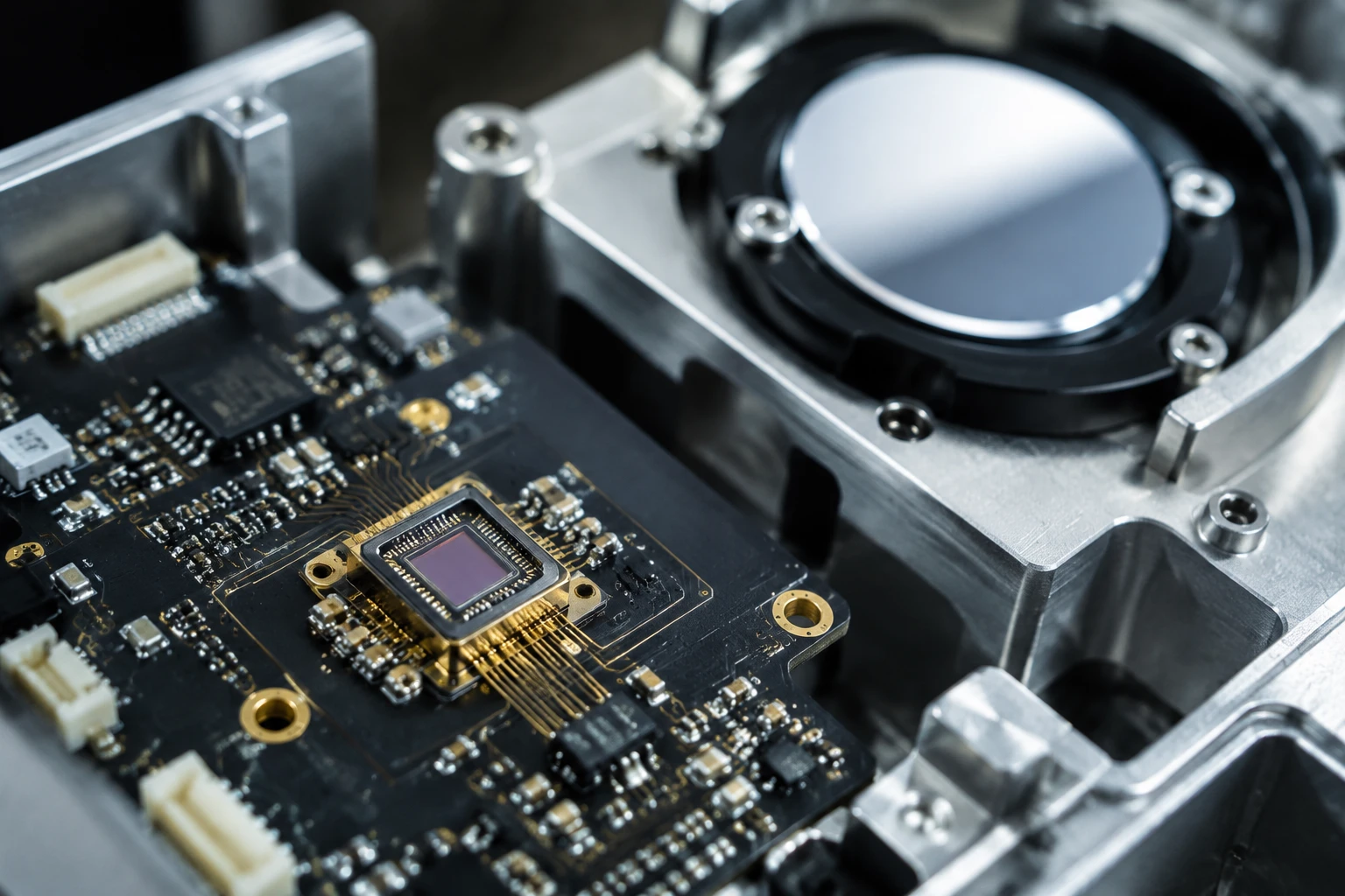
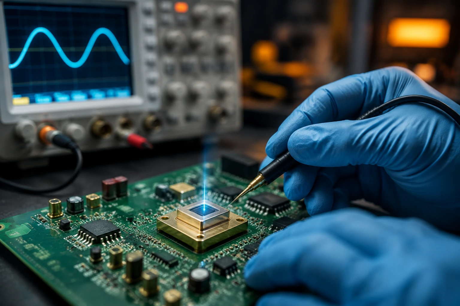
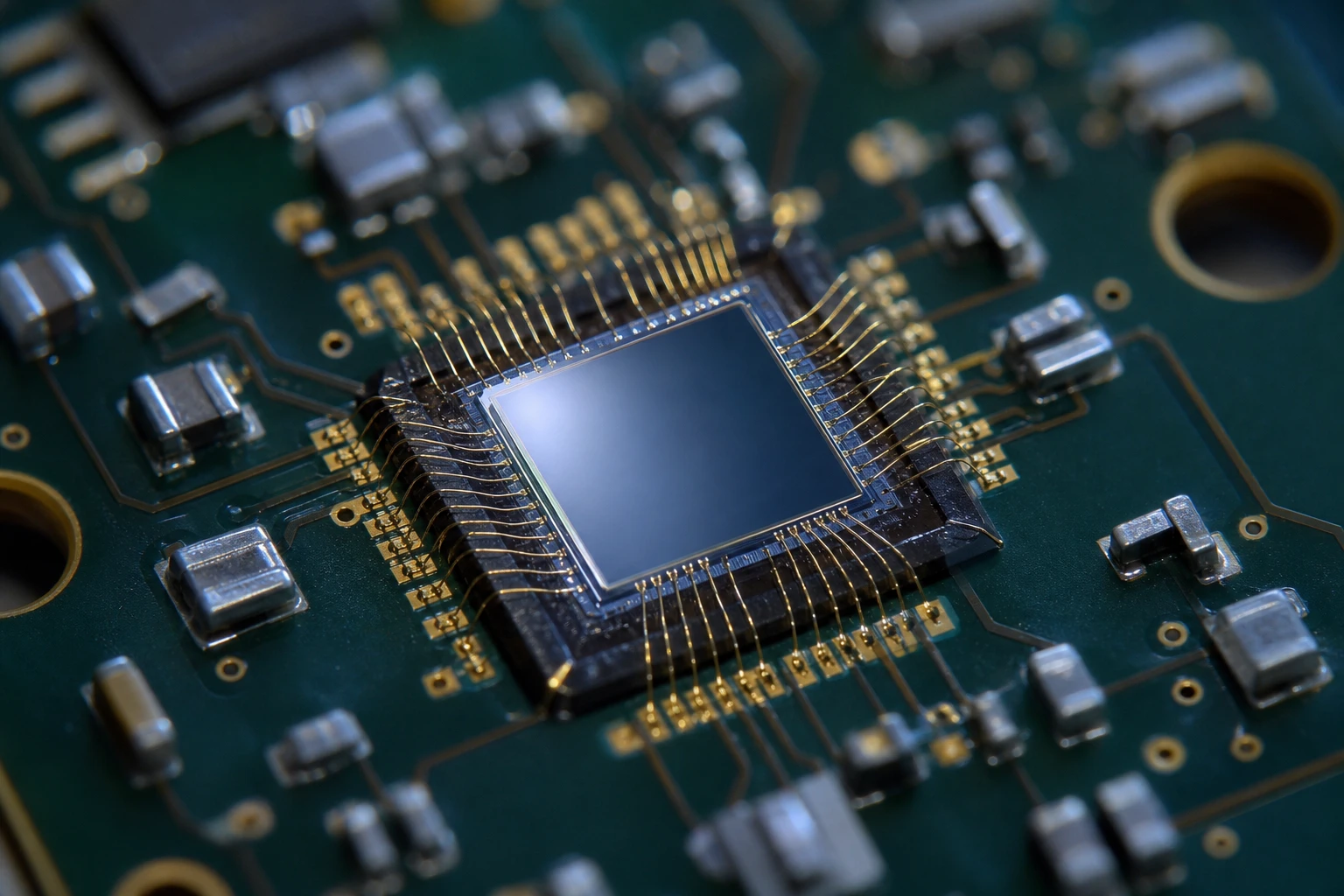
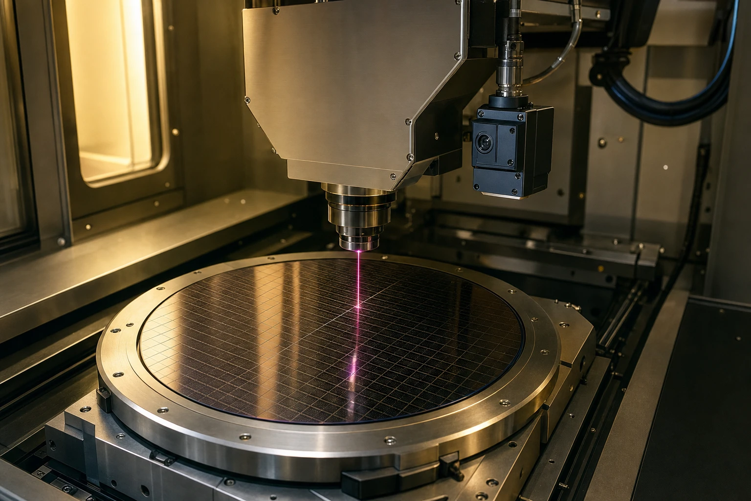
I’ve spent the better part of the last decade hunched over oscilloscopes, trying to figure out why a perfectly good simulation fails in the real world. More often than not, the solution lies in smart photo IC integration. Unlike the old days of discrete photodiodes and separate amplifiers, Photo ICs (Integrated Circuits) pack the detector, amplifier, and signal processing logic into one tiny package.
But here is the thing nobody tells you: just because it is integrated doesn’t mean it is “plug and play.” You can’t just slap it on a PCB and expect magic.
In this guide, I’m going to walk you through the gritty details of photo IC integration. We are going to talk about optical sensor circuit design, dealing with noise, and how to actually get these things to perform in compact industrial housings without losing your mind.
Why Bother with Photo ICs?
Before we dive into the “how,” let’s briefly touch on the “why.” If you are building legacy equipment, discrete components are fine. But for modern compact industrial sensors, space is a luxury you don’t have.
Photo IC integration solves three massive headaches:
- Space: You replace 3-5 components with one.
- Noise: The high-impedance wiring (the scary part) is sealed inside the chip.
- Cost: Less pick-and-place time on the assembly line.
I remember working on a project for a bottling plant. We tried using a discrete photodiode + transimpedance amp. The EMI from the conveyor motors killed our signal. It was a disaster. We switched to a Photo IC from BeePhoton’s category and the noise floor dropped by like 20dB instantly. Lesson learned.
The Core Challenge: Optical Sensor Circuit Design in Tight Spaces
When you are doing photo IC integration in a housing the size of a USB stick, your biggest enemy isn’t the circuit—it’s the layout.
1. The Decoupling Capacitor Rule (Do Not Ignore This)
This sounds basic, but I see senior engineers mess this up. A Photo IC is an active device. It has an internal amplifier. Amplifiers hate power supply ripple.
You need a bypass capacitor. But not just anywhere. It needs to be physically touching the Vcc and GND pins if possible.
- Recommendation: Use a 0.1 uF ceramic capacitor (X7R dielectric is best for industrial temps).
- Placement: If your trace length from the pin to the cap is more than 5mm, you are asking for trouble.
2. Grounding Strategies for Miniaturized Sensors
In miniaturized sensors, you don’t have room for massive ground planes. But you need to create a “quiet zone” for the optical sensor.
- Star Grounding: Run a separate ground trace for the Photo IC back to the main power entry point. Don’t daisy chain it with the noisy LED driver or the IO-Link transceiver.
- Thermal Relief: These chips can get warm. Ensure your ground pad acts as a heatsink, even if it’s small.
3. Avoiding Optical Crosstalk
This isn’t an electrical issue, but it ruins optical sensor circuit design constantly. When you shrink the housing, the LED emitter sits right next to the Photo IC receiver.
If you don’t optically isolate them, light will bleed internally through the PCB material (FR4 is translucent!) or bounce off the cover glass.
- Hack: Cut a slot in the PCB between the emitter and the Photo IC.
- Hack 2: Use a black soldermask. Green soldermask reflects light; black absorbs it.

Photo IC PDTC series
Our Two-level Gain Switch Photo IC provides precise optical detection for industrial automation. This advanced photo IC features an adjustable gain switch, ensuring reliable performance
Calculating Gain and Bandwidth (Text-Friendly Math)
Okay, since we are using the WordPress Visual Editor here, I’m not going to throw complex LaTeX code at you. Let’s keep the math simple and text-based so you can copy-paste this into your engineering notes.
When you are selecting a component for photo IC integration, you usually look at the sensitivity. But you need to match this to your ADC (Analog-to-Digital Converter) range.
The Voltage Output Formula
Most analog output Photo ICs follow this logic:
V_out = P_in * S
Where:
- V_out: Output Voltage (Volts)
- P_in: Input Optical Power (Watts)
- S: Sensitivity (Volts/Watt)
If you are using a Photo IC with a built-in Transimpedance Amplifier (TIA), the sensitivity is a product of the photodiode responsiveness and the feedback resistor.
S = R_lambda * R_f
Where:
- R_lambda: Photo sensitivity (Amps/Watt), usually around 0.4 to 0.6 A/W for silicon at 850nm.
- R_f: Internal Feedback Resistor (Ohms).
Example:
You have a Photo IC with a sensitivity of 0.5 A/W and an internal gain resistor of 100k Ohms. You receive 5 microwatts (uW) of light.
- Convert uW to Watts: 5 uW = 0.000005 W
- Calculate V_out:
V_out = 0.000005 W * 0.5 A/W * 100,000 Ohms
V_out = 0.25 Volts
If your ADC reference is 3.3V, 0.25V is a bit low. You might need a Photo IC with higher gain or add an external gain stage. This is a crucial step in photo IC integration.
Bandwidth Trade-off
Here is the catch: The higher the gain (R_f), the lower the bandwidth. It’s the laws of physics.
f_c = 1 / ( 2 * pi * R_f * C_f )
- f_c: Cutoff frequency (-3dB point)
- pi: 3.14159…
- C_f: Feedback capacitance (parasitic + intentional).
If you are designing a high-speed counter sensor, don’t pick a Photo IC with massive gain. It will be too slow.
Photo IC vs. Discrete Components: A Reality Check
I get asked this a lot by clients at BeePhoton. “Why should I buy a Photo IC when I can buy a photodiode for 10 cents?”
Valid question. But let’s look at the hidden costs.
| Feature | Discrete Photodiode Design | Photo IC Integration |
|---|---|---|
| PCB Real Estate | High (Diode + OpAmp + Passives) | Ultra-Low (Single Chip) |
| Noise Immunity | Poor (Traces pick up EMI) | Excellent (Shielded internally) |
| Design Time | High (Need to tune stability) | Low (Pre-tuned) |
| Component Count | 5-8 parts | 1-2 parts |
| Cost | Low BOM, High Assembly/Testing | Moderate BOM, Low Assembly |
For miniaturized sensors, the Photo IC wins every time simply because you cannot physically fit the discrete circuit without compromising performance.
Photo IC PDTC series
Our Two-level Gain Switch Photo IC provides precise optical detection for industrial automation. This advanced photo IC features an adjustable gain switch, ensuring reliable performance
Troubleshooting: Why Is My Sensor Acting Weird?
So, you’ve done your photo IC integration, sent the Gerber files out, got the boards back, and… the signal is jumping all over the place.
Here is my “First Aid” checklist for optical sensor circuit design issues:
1. The “Sunlight” Problem
Did you forget the optical filter? Photo ICs are sensitive. If you are using an 850nm LED (Infrared), but your sensor is getting hit by sunlight or factory LED lighting, it saturates.
- Fix: Use a Photo IC with a built-in daylight filter or add a physical IR-pass filter lens.
2. Power Supply Ripple
I once debugged a sensor where the output oscillated at 100kHz. Turns out, the switching regulator powering the board was operating at… you guessed it, 100kHz.
- Fix: Add a ferrite bead in series with the Vcc pin of the Photo IC. It kills high-frequency noise dead.
3. Soldering Stress
This is a weird one. Miniaturized sensors use tiny plastic lenses. If you reflow the PCB at too high a temperature, the clear epoxy on the Photo IC can yellow or cloud up.
- Fix: Check the datasheet for the reflow profile. Don’t cook your chips.
Real World Case Study: The “Ghost” Object
I want to share a story (names changed to protect the innocent) about a project involving photo IC integration for a warehouse robot.
The Problem:
The client was building a collision detection sensor. They used a generic Photo IC. The robot kept stopping when nothing was there. We call this “ghosting.”
The Investigation:
I flew out to their facility. We opened up the sensor. They had routed the output trace of the Photo IC directly underneath a high-current motor driver chip on the other side of the PCB.
Even though it was a digital output Photo IC, the inductive spike from the motor was coupling into the trace, flipping the bit from 0 to 1.
The Solution:
- We moved the Photo IC trace to an inner layer, sandwiched between two ground planes.
- We switched to a BeePhoton differential output Photo IC, which is way more robust against common-mode noise.
The Result:
False triggers went to zero. The client was happy, and I got a free lunch. This highlights that photo IC integration isn’t just about the schematic; it’s about the physical reality of the PCB.
Selecting the Right Photo IC for Your Application
At BeePhoton, we see all kinds of crazy applications. But usually, photo IC integration falls into three buckets:
1. The Simple Switch (Presence/Absence)
You just need a digital High/Low. Is the box there? Yes or No.
- Look for: “Digital Output Photo IC” or “Optical Switch.”
- Key spec: Threshold irradiance.
2. Distance Measurement (Triangulation)
You need to know how far the object is.
- Look for: PSD (Position Sensitive Detector) integrated ICs. These are complex but give you analog voltage based on where the light hits the chip.
3. Ambient Light Sensing
You want to dim a display based on room brightness.
- Look for: Linear output Photo ICs with human eye spectral response.
Photo IC PDTC series
Our Two-level Gain Switch Photo IC provides precise optical detection for industrial automation. This advanced photo IC features an adjustable gain switch, ensuring reliable performance
Future-Proofing Your Design
Miniaturized sensors are only getting smaller. We are seeing a trend where the Photo IC is being integrated directly into the connector or the cable head.
If you are starting a new optical sensor circuit design today, think about thermal management. As chips get smaller, they get hotter. Ensure your photo IC integration plan includes a way to get heat out of the package, or your sensitivity will drift like a boat without an anchor.
Also, don’t be afraid to ask for help. We love geeky engineering questions at BeePhoton. If you are stuck on a gain calculation or a noise issue, reach out to us. We’ve probably seen it before.
Conclusion
Photo IC integration is the secret weapon for building modern, miniaturized sensors. It saves space, kills noise, and makes your life easier—if you follow the rules.
Remember:
- Decouple your power supply close to the pin.
- Watch out for optical crosstalk in the PCB.
- Calculate your gain vs. bandwidth trade-off carefully.
Your industrial clients don’t care about how hard the design was; they just want a sensor that works when the machinery is vibrating and the lights are flickering. Using a quality Photo IC is the best way to deliver that.
Ready to upgrade your sensor design?
Stop fighting with discrete components.
Check out our full range of Photo ICs here: https://photo-detector.com/product-category/photo-ic/
Or, if you have a specific technical challenge and need a second pair of eyes on your schematic, drop us a line. We are actual engineers, not just salespeople.
Contact BeePhoton: https://photo-detector.com/contact-us/
Email: info@photo-detector.com
FAQ: Photo IC Integration
Q1: What is the biggest mistake engineers make with photo IC integration?
A: Ignoring the optical layout. Engineers often focus purely on the electrical side (schematics) and forget that light needs to travel cleanly. If you don’t use barriers or proper housing materials to prevent light from the emitter leaking directly into the Photo IC (crosstalk), no amount of circuit tweaking will fix the sensor. It is a mechanical issue as much as an electrical one.
Q2: Can I use a Photo IC for high-speed fiber optic communications?
A: generally, no. The Photo ICs used in industrial sensors are optimized for sensitivity and robustness, not extreme speed. Industrial Photo ICs typically operate in the kHz to low MHz range. For fiber optics (Gigabit speeds), you need specialized high-speed photodiodes and transimpedance amplifiers, which are a different beast entirely. Always check the “Rise Time” and “Fall Time” in the datasheet.
Q3: How does temperature affect photo IC integration?
A: Temperature is a silent killer. As temperature rises, the “Dark Current” (noise) of the photodetector increases, and the spectral sensitivity can shift. In miniaturized sensors, heat gets trapped easily. When designing, ensure your photo IC integration allows for some thermal dissipation (ground planes help). If your environment is over 85°C, make sure you select an automotive or industrial-grade chip, not a consumer-grade one.