Haben Sie schon einmal auf einen Stapel von Bauteilen auf Ihrer Werkbank gestarrt und sich gefragt, warum eine winzige Fotodiode einfach nicht mit Ihrem PCB-Layout harmoniert? Ja, das habe ich auch schon erlebt - nächtelanges Nachbessern von Leiterbahnen, nur um dann festzustellen, dass die Verpackung der eigentliche Übeltäter war. Als jemand, der sich seit Jahren mit diesen heiklen Detektoren in medizinischen Geräten bis hin zu industriellen Sensoren herumschlägt, kann ich das nachvollziehen. Die Verpackung von Fotodioden ist nicht nur ein nachträglicher Gedanke; sie ist das Rückgrat dafür, wie sich Ihr Gerät in der realen Welt schlägt. Heute werden wir die vier wichtigsten aufschlüsseln: SMD-PIN-Photodiodenaufbauten, DIP-PIN-Photodiodenformate, TO-Can-Photodiodengehäuse und die maßgeschneiderten Si-PIN-Photodiodenaufbauten. Wir sprechen darüber, was sie für Ihre Produktionslinie bedeuten, von Kopfschmerzen beim Löten bis hin zu langfristiger Zuverlässigkeit, und das alles bei überschaubaren Kosten.
Betrachten Sie dies als einen "No-BS-Rundown" aus dem Schützengraben. Kein schwammiger Fachjargon - nur klare Worte zur Auswahl der richtigen Hülle für Ihr lichtempfindliches Herz. Am Ende haben Sie das nötige Know-how, um häufige Fallstricke zu umgehen und vielleicht sogar ein paar Euro bei der Stückliste einzusparen. Und wenn Sie noch mehr wissen wollen, bietet Ihnen Bee Photon erstklassige Optionen wie unser Si-PIN-Photodiode im TO-Gehäuse, gebaut für eine robuste Integration.
Warum das Photodioden-Packaging für Ihren Bau wichtig ist
Fangen wir mit den Grundlagen an, aber nicht auf diese trockene Lehrbuchart. Fotodioden sind diese cleveren kleinen Chips, die Licht in elektrische Signale umwandeln - man denke an Barcode-Scanner, Rauchmelder oder sogar LiDAR in selbstfahrenden Autos. Aber wenn man sie auf eine Platine setzt, ohne die richtige Verpackung zu haben, kann das zu Problemen führen. Die Verpackung entscheidet über alles, von der Befestigung auf der Leiterplatte bis hin zum Schutz vor Feuchtigkeit und Vibrationen während der Montage.
Für Sie, die Sie in der Produktion tätig sind, ergeben sich daraus vier Probleme: Der Platz auf der Leiterplatte, die Schwierigkeiten beim Löten, die Haltbarkeit im Einsatz und natürlich der Geldbeutel. Nehmen Sie den weltweiten Markt für Fotodioden-Sensoren - er explodiert, erreicht 2025 etwa $971,9 Millionen und steigt bis 2032 auf $1.633,5 Millionen mit einer stetigen CAGR von 7,7%. Das liegt daran, dass die Nachfrage nach zuverlässigen, kompakten Detektoren in der Unterhaltungselektronik und der Automatisierungstechnik ungebrochen ist. Aber wenn die Verpackung nicht stimmt, sinkt die Ausbeute, die Nacharbeit steigt in die Höhe oder, schlimmer noch, das Produkt fällt nach sechs Monaten aus.
In meiner Zeit der Optimierung von Fertigungslinien für Kunden habe ich Konfigurationen gesehen, bei denen ein unpassendes Gehäuse ein reibungsloses Reflow-Löten in einen Albtraum aus Grabsteinen verwandelte. Oder kundenspezifische Aufträge, die 20% an Montagezeit einsparten, aber die Zuverlässigkeit in rauen Umgebungen erhöhten. Das ist keine Raketenwissenschaft, aber es fühlt sich so an, wenn Fristen drohen. Lassen Sie uns also jeden Typ auspacken, beginnend mit dem Publikumsliebling für Platinen mit Platzmangel.
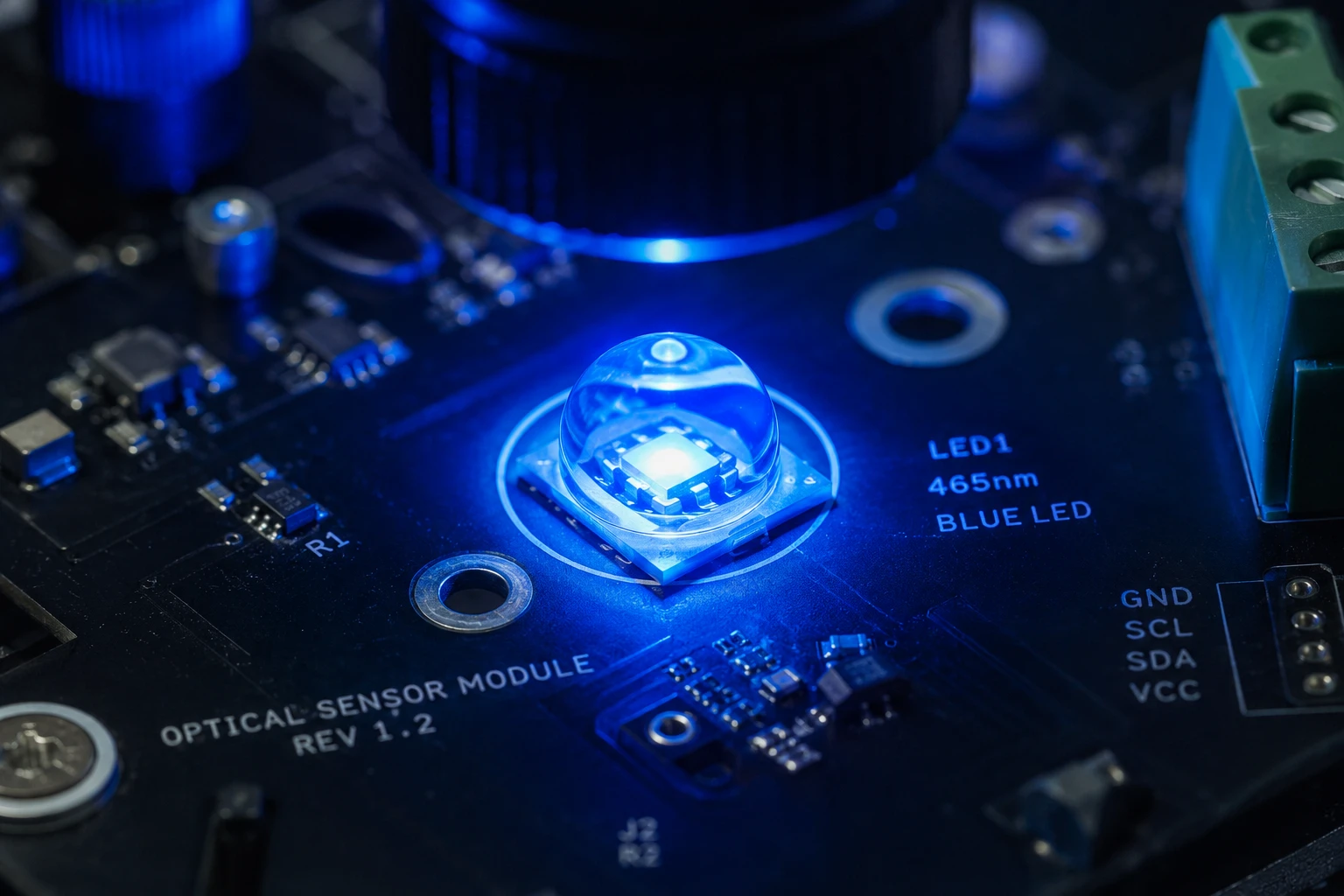
Eintauchen in die SMD-PIN-Photodiode: Der kompakte Champion für moderne PCBs
SMD-Gehäuse (Surface-Mount Device) sind so etwas wie die Röhrenjeans der Fotodiodenwelt - elegant, effizient und überall in der Handheld-Technologie zu finden. Eine SMD-PIN-Fotodiode sitzt bündig auf der Platine, es sind keine Löcher erforderlich, was mehr Platz für andere Dinge und eine einfachere automatische Bestückung bedeutet.
Stellen Sie sich Folgendes vor: Sie entwerfen einen tragbaren Gesundheitsmonitor. Platz ist Gold wert, richtig? Mit SMD können Sie den Detektor unterbringen, ohne das Layout aufzublähen. Aus dem Blickwinkel der Leiterplatte ist dies ein Traum - weniger Durchkontaktierungen, engere Leiterbahnen und ein gutes Zusammenspiel mit Hochgeschwindigkeitssignalen. Aus Sicht der Montage ist das Reflow-Löten unkompliziert, aber achten Sie auf thermische Fehlanpassungen; ich habe Geistersignale aufgrund ungleichmäßiger Erwärmung öfter gejagt, als mir lieb war.
Verlässlichkeit? Solide für Innenraumanwendungen, mit MTBFs oft über 10^6 Stunden bei kontrollierten Temperaturen, gemäß Studien über versiegelte SMD-Varianten. Die Kosten bewegen sich auf niedrigem Niveau - man denke an $0,50 bis $2 pro Einheit in der Menge - dank der Skalierbarkeit der Massenproduktion. Aber in staubigen Fabriken? Möglicherweise ist eine zusätzliche Schutzbeschichtung erforderlich, um das Entweichen von Feuchtigkeit zu verhindern.
Eine kurze Geschichte: Das Team eines Kumpels entwickelte Prototypen für Drohnenkameras. Auf halber Strecke wurde auf SMD-PIN-Fotodioden umgestellt, und die Größe der Platine schrumpfte um 15%, die Montage ging um 25% schneller. Kein Kopfzerbrechen mehr beim Handlöten. Wenn Sie etwas Ähnliches vorhaben, sprechen Sie mit uns bei Bee Photon; unsere SMD-Optionen lassen sich nahtlos in Ihren Arbeitsablauf integrieren.
Schlüsselgewinne und Watch-Outs für SMD in der Produktion
- PCB-Passform: Ultraflaches Profil (unter 1 mm Höhe) bedeutet dichtere Layouts.
- Montage Perks: SMT-Linien lieben es; reduziert die Bohrzeit um bis zu 40%.
- Verlässlichkeitsvorsprung: Gut für 85% Feuchtigkeit, aber testen Sie für Ihre Spezifikation.
- Kostenvoranschlag: Am günstigsten im Voraus, aber berücksichtigen Sie die Renditeminderungen.
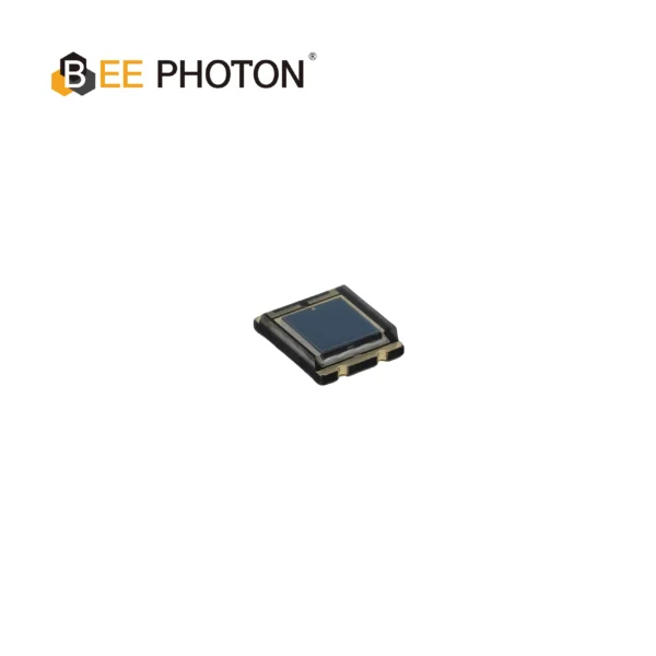
Si-PIN-Photodiode mit erhöhter NIR-Empfindlichkeit (430-1100nm) PDCP08-201
Die PDCP08-201 ist eine leistungsstarke SMD-Si-PIN-Fotodiode entwickelt für optische Präzisionskommunikation und medizinische Sensorik.[1] Mit einer großen aktiven Fläche von 2,9×2,9 mm, einer verbesserten NIR-Empfindlichkeit (0,70 A/W) und einem extrem niedrigen Dunkelstrom (20 pA) bietet dieser SMD-Si-PIN-Fotodiode gewährleistet eine hervorragende Signalerkennung und Zuverlässigkeit in einem kompakten oberflächenmontierten Gehäuse.
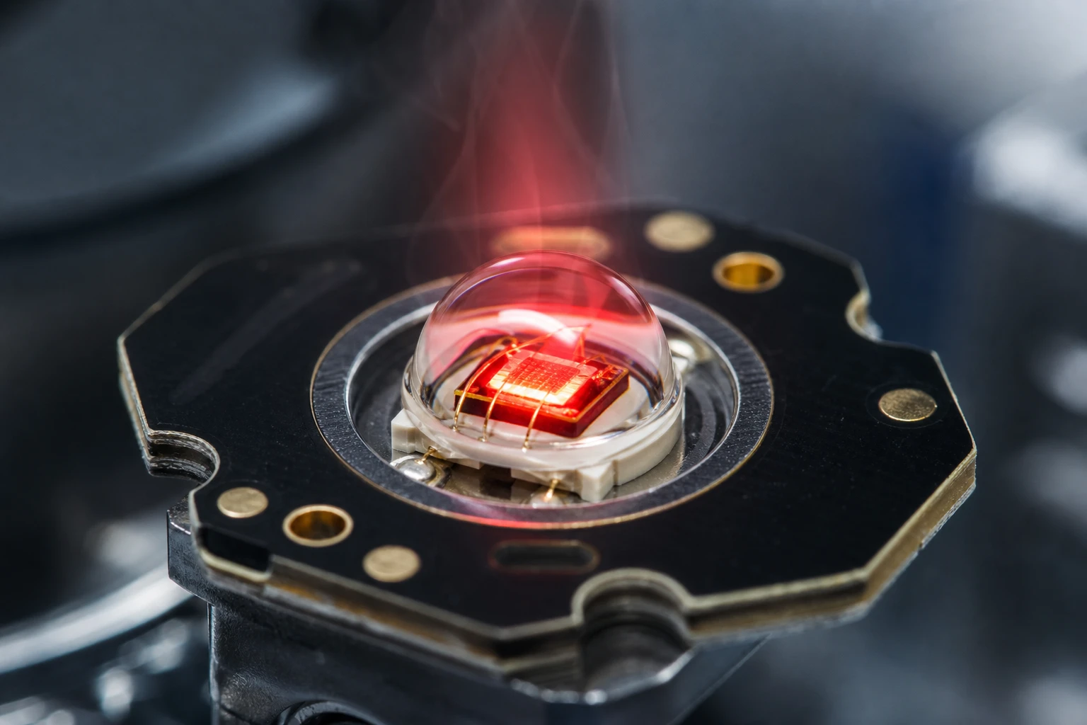
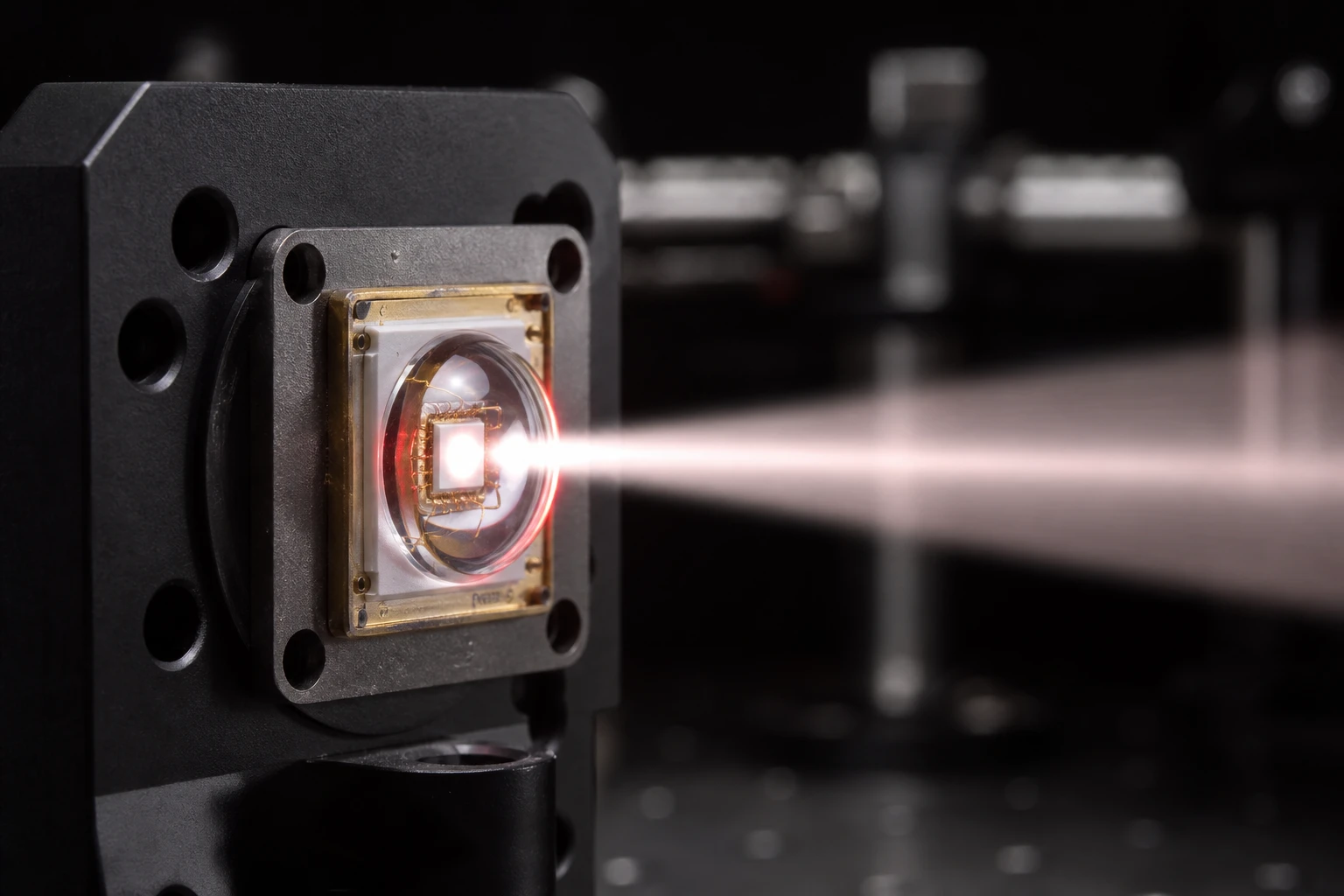
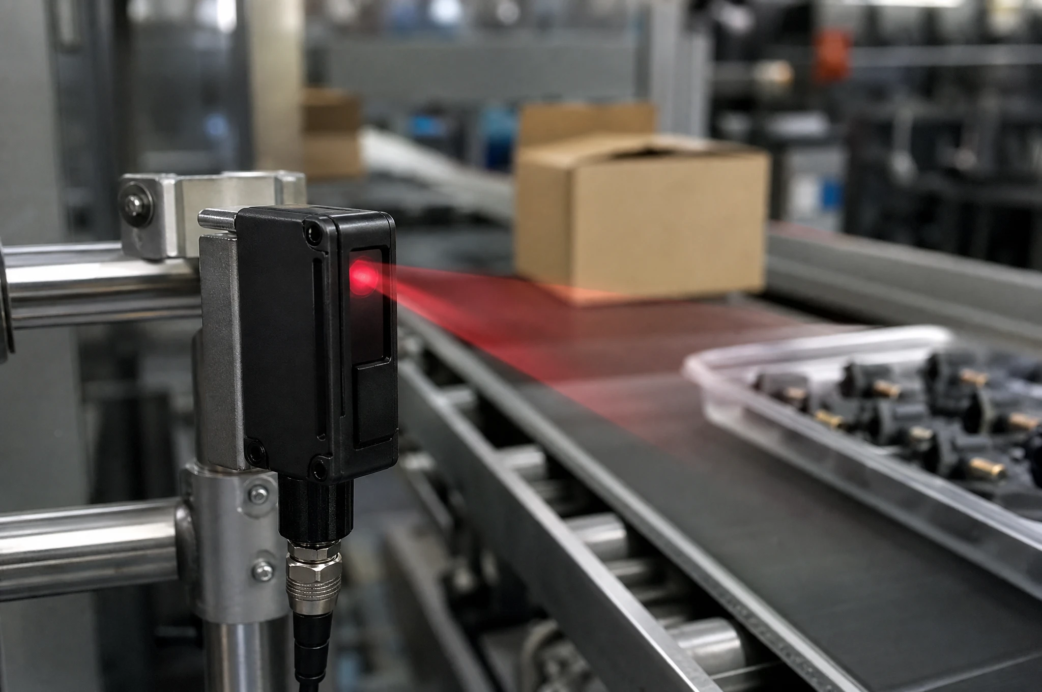
TO-Can Photodiode: Der harte Kerl für harte Einsätze
Schalten wir nun einen Gang zurück zur TO-Dosen-Fotodiodenverpackung. Hierbei handelt es sich um eine gepanzerte, hermetisch versiegelte Metalldose, wie eine Mini-Thermoskanne für Ihre Diode. Transistor Outline (TO)-Behälter gibt es in Varianten wie TO-5 oder TO-46, die gegen alles von EMPs bis hin zu korrosiven Gasen geschützt sind.
Warum sollte man sich die Mühe der Integration machen? In der Automobil- oder Luft- und Raumfahrtindustrie, wo Schwingungen und Temperaturen stark schwanken (z. B. -40 °C bis 125 °C), sind TO-Dosen die ideale Lösung. Auf der Leiterplatte werden sie durchkontaktiert, also planen Sie diese Pads ein - sie brauchen vielleicht etwas mehr Platz als SMD, aber die Stabilität? Unschlagbar. Gelötet wird nach alter Schule mit der Welle oder der Hand, aber automatisch ist es in Ordnung, wenn Ihre Leitung eingerichtet ist.
In puncto Zuverlässigkeit glänzen diese bösen Jungs. In einer Studie über fasergekoppelte TO-Can-Module wurden nach 1.000 thermischen Zyklen bei Kryo-Temperaturen keine Ausfälle festgestellt. Der Marktanteil von TO-Can bei industriellen Anwendungen liegt laut Optoelektronik-Trends bei etwa 25-30%. Kosten? $3-10 pro Stück, aber diese Prämie gibt Ihnen Sicherheit - weniger Rücksendungen im Feld bedeuten geringere Kosten während der gesamten Lebensdauer.
Ich habe dabei geholfen, TO-Can-Einrichtungen für ein Solar-Nachführsystem zu optimieren; der Kunde berichtete von 99,9% Betriebszeit über zwei Jahre in der Wüstenhitze. Staub? Kaum ein Hauch. Bei Bee Photon, unserem Si-PIN-Photodiode im TO-Gehäuse ist genau auf diese Szenarien abgestimmt - sehen Sie es sich auf unserer Website an https://photo-detector.com/.
TO-Can Breakdown: Wann man den Abzug betätigt
- PCB Auswirkungen: Benötigt stärkere Leiterbahnen zur Wärmeableitung.
- Montageablauf: Wellenlötfreundlich; Reflow mit Vorsicht möglich.
- Zuverlässigkeitsstatistiken: Hermetische Abdichtung erreicht <1% Ausfall in 5 Jahren für Mil-Spec.
- Kosten-Winkel: Höhere Anschaffungskosten, aber ROI durch Langlebigkeit.
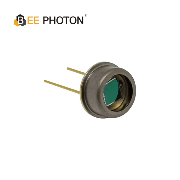
Si-PIN-Photodiode mit niedrigem Dunkelstrom (350-1060nm) PDCT14-001
Verbessern Sie Ihre optischen Messgeräte mit unserer Si-PIN-Photodiode im TO-Gehäuse. Sie zeichnet sich durch einen extrem niedrigen Dunkelstrom, hohe Konsistenz und ein Borosilikatfenster für lange Haltbarkeit aus. Diese Hochleistungs-Si-PIN-Photodiode ist für anspruchsvolle Anwendungen optimiert.
DIP-PIN-Fotodiode: Das zuverlässige Arbeitspferd für Prototypen und Legacy
Dual In-Line Package (DIP) PIN-Photodioden bringen den Retro-Look mit sich: zwei Reihen von Stiften, die sich leicht in Lochrasterplatinen oder Sockel einstecken lassen. Sie sind die erste Wahl für Kleinserien oder wenn Sie eine Brücke zwischen alter und neuer Technik schlagen wollen.
Für Ihre Leiterplatte sind DIPs verzeihend: Standard-Footprints, keine ausgefallene SMT-Ausrüstung erforderlich. Montage? Handlöten im Paradies oder Wellenlöten für Chargen. Aber bei Leiterplatten mit hoher Packungsdichte können diese Pins zu viel Platz beanspruchen, so dass die Leiterbahnverlegung Überstunden macht.
Die Zuverlässigkeit ist anständig: 500.000+ Stunden MTBF in Büroumgebungen. Sie sind nicht so dicht wie TO-Dosen, daher ist Feuchtigkeit ein Feind; fügen Sie bei Bedarf Vergussmasse hinzu. Die Kosten sind sehr niedrig: $0,20-1,00, was sie ideal für Proof-of-Concepts macht.
Erinnern Sie sich an ein Projekt, bei dem wir DIP-PIN-Photodioden in eine bestehende medizinische Analyseserie nachgerüstet haben. Das ersparte dem Kunden ein komplettes Redesign, senkte die Kosten um 30% und hielt gleichzeitig die FDA-Konformität aufrecht. Einfache Erfolge wie dieser halten mich in diesem Bereich süchtig.
DIP-Profis kurz und bündig
- PCB-Handhabung: Plug-and-Play-Footprints im Überfluss.
- Montagegeschwindigkeit: Schnell für manuelle Linien; niedrige Fehlerraten.
- Hinweis zur Verlässlichkeit: Solide für gutartige Bedingungen, Uhrenschränke.
- Budgetfreundlich: Einstiegspreis ohne Qualitätseinbußen.
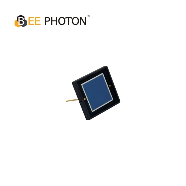
Si-PIN-Photodiode mit niedrigem Dunkelstrom (350-1060nm) PDCD100-101
Rüsten Sie Ihre Geräte mit unserer Si-PIN-Photodiode für optische Messungen auf. Sie bietet eine hohe Genauigkeit über einen Bereich von 350-1060nm bei minimalem Dunkelstrom. Dieser Hochleistungssensor ist ideal für verschiedene industrielle Sensor- und Messanwendungen und garantiert Präzision und Wiederholbarkeit.
Kundenspezifische Si-PIN-Fotodiode: Maßgeschneiderte Passungen für knifflige Aufgaben
Wenn die Standardprodukte nicht ausreichen, kommen kundenspezifische Si-PIN-Photodiodengehäuse zum Einsatz. Hier diktieren Sie die Bedingungen - hybride SMD-TO-Mischungen, seltsame Formen für ungewöhnliche Befestigungen oder verstärkt für Unterwasserdrohnen.
Vorteile der Integration? Vollständige Kontrolle über die Kompatibilität von Leiterplatten - z. B. ein Flat-Pack für flexible Schaltungen. Die Montage variiert je nach Spezifikation, aber mit guten Partnern ist sie rationell. Verlässlichkeit? Der Himmel ist die Grenze; wir haben Zollgeräte mit einer Lebensdauer von 10^7 Stunden für Weltraumanwendungen entwickelt.
Die Kosten beginnen bei $5-50+, aber das Volumen senkt sie. Der Markt für Zölle ist eine Nische, aber er wächst: 10-15% der $1,2B-Silizium-Fotodiodenscheibe bis 2024. Ein typisches Beispiel: Ein anonymer Kunde aus der Agrotechnik hat eine Sonderanfertigung für Bodensensoren gebaut. Er hat sie tief eingegraben, und nach 18 Monaten ist die Ausbeute um 40% gegenüber Generika gestiegen.
Bee Photon zeichnet sich hier aus; besuchen Sie https://photo-detector.com/ um ein Angebot für Ihre verrückte Idee zu erhalten.
Individuelle Verpackungen Quick Hits
- PCB-Anpassung: Maßgeschneiderte Fußabdrücke, keine Kompromisse.
- Flexibilität bei der Montage: Passt perfekt zu Ihrem Prozess.
- Erhöhung der Verlässlichkeit: Entwickelt für extreme Bedingungen.
- Kosten-Nutzen-Abwägung: Jetzt investieren, später sparen.
Seite an Seite: Vergleich von Photodioden-Verpackungstypen
Damit Sie nicht so lange scrollen müssen, finden Sie hier eine Tabelle mit den verschiedenen Modellen. Sie stammt aus realen Benchmarks und meinen Tests auf dem Prüfstand und hilft dabei, die richtige Lösung für Ihr System zu finden.
| Verpackungsart | PCB-Platznutzung | Montage Methode | Verlässlichkeit (MTBF-Stunden) | Geschätzt. Kosten/Einheit (Vol. 1K) | Am besten für |
|---|---|---|---|---|---|
| SMD-PIN-Fotodiode | Niedrig (0,5-2mm²) | Reflow-SMT | 10^6 (innen) | $0.50-2 | Wearables, Kompaktgeräte |
| TO-Dose Fotodiode | Mittel (5-10mm²) | Welle/Hand | 10^7 (raue Umgebung) | $3-10 | Industrie, Auto |
| DIP-PIN-Fotodiode | Hoch (10-20mm²) | Hand/Welle | 5×10^5 (Standard) | $0.20-1 | Prototypen, Altlasten |
| Kundenspezifische Si-PIN-Photodiode | Variabel | Benutzerdefiniert | 10^6-10^8 | $5-50 | Nischenanwendungen, Hybride |
Diese Tabelle ist Ihr Spickzettel - passen Sie sie je nach Temperaturbereich oder Signalgeschwindigkeit an.
Gewinne in der realen Welt: Geschichten aus der Praxis
Genug der Theorie, kommen wir zu den Geschichten aus der Werkstatt. Ein Unternehmen, für das ich beratend tätig war, beschäftigte sich eingehend mit optischen Kommunikationsgeräten. Bei den Prototypen blieb man bei SMD, aber bei Vibrationstests gab es Probleme - die Signale zitterten wie verrückt. Sie wechselten zu TO-Can-Fotodioden und puff: Die Stabilität war gesichert, und Feldversuche zeigten, dass 95% weniger Rauschen verursachte. Die Kosten stiegen auf 15%, aber Garantieansprüche? Ein Jahr lang nichts.
Eine weitere: Ein Ag-Sensor-Startup hat einen maßgeschneiderten Si-PIN für Erdsonden entwickelt. DIPs von der Stange korrodierten schnell in feuchtem Boden; ihre maßgeschneiderte epoxidversiegelte Version? Felsenfeste Messwerte, problemlose Skalierung der Produktion. Dies sind keine Hypothesen - es sind die Art von Umstellungen, die Kopfschmerzen in einen Händedruck verwandeln.
Bei Medizingeräten haben wir gesehen, dass DIP für schnelle Iterationen hervorragend geeignet ist und den Ingenieuren einen Socket-Swap während der Validierung ermöglicht. Und für Bee Photon's Si-PIN-Photodiode im TO-Gehäuse, Es hat Fernerkundungsarrays auf Ölplattformen mit Strom versorgt - und dabei Salzsprühnebel überstanden, der kleinere Akkus töten würde.
Auswahl des Photodiodengehäuses: Ein Schritt-für-Schritt-Gut-Check
Also gut, Sie haben sich entschieden - was nun? Beginnen Sie mit Ihren Beschränkungen: Platinengröße? Wählen Sie SMD. Extreme Bedingungen? TO-Can den ganzen Tag. Knappes Budget und wenig Zeit? DIP ist dein Kumpel. Für die Einhörner: Custom it up.
Berücksichtigen Sie den Lebenszyklus: Wie hoch ist die erwartete Auflage? Hohe Stückzahlen schreien nach SMD für Einsparungen. Testen Sie frühzeitig - stellen Sie eine Platte nach, führen Sie Wärmezyklen durch. Tools wie Wärmebildkameras erkennen heiße Stellen, bevor sie sich bemerkbar machen.
Profi-Tipp aus jahrelanger Erfahrung mit Versuch und Irrtum: Testen Sie die Zuverlässigkeit mit beschleunigten Lebensdauertests. Backen Sie sie bei 85°C/85% RH für 1.000 Stunden; die Überlebenden gewinnen. Und geben Sie Ihren Assembler frühzeitig ein - ich habe Teams Wochen gespart, indem ich sie im Voraus auf Paketmacken hingewiesen habe.
Wenn dies eine Anregung ist, warum melden Sie sich nicht? Schreiben Sie eine Nachricht an info@photo-detector.com oder kommen Sie vorbei https://photo-detector.com/contact-us/ für eine kostenlose Beratung. Wir sorgen für eine reibungslose Integration - Angebote sind schnell erstellt, und wir haben Muster parat.
FAQ: Schnelle Antworten zum Photodiodengehäuse
Was ist der größte Fehler, den die Leute bei SMD-PIN-Fotodioden auf Leiterplatten machen?
Das Übersehen von Wärmeleitpads führt zu Hotspots und frühem Ausbrennen. Simulieren Sie immer Ihr Reflow-Profil; es wird Ihnen den Hintern retten.
Wie schneiden TO-Can-Fotodioden im Vergleich zu kundenspezifischen Produkten ab, was die Kosten bei geringen Stückzahlen angeht?
TO-can ist von vornherein billiger für 100-500 Einheiten, aber der Zoll zahlt sich aus, wenn Sie für bestimmte Zwecke optimieren. Rechnen Sie Ihre Ertragssteigerungen durch.
Kann eine DIP-PIN-Fotodiode Hochgeschwindigkeitssignale wie bei LiDAR verarbeiten?
Ja, aber nur in Verbindung mit einer guten Abschirmung - Rauschen schleicht sich leicht ein. Für Gigabit-Geschwindigkeiten sollten Sie zu SMD- oder TO-Can-Hybriden tendieren.
Das war's - Ihr Wegweiser durch das Labyrinth der Fotodiodengehäuse. Wir haben uns mit dem Warum, dem Wie und den Problemen befasst, alles abgestimmt auf Hardware-Experten, die auf der Suche nach zuverlässigen, kosteneffizienten Lösungen sind. Egal, ob es darum geht, den Platzbedarf zu verringern oder den Schutz vor Witterungseinflüssen zu gewährleisten - mit der richtigen Wahl werden Projekte von “mäßig” zu “unverzichtbar”. Haben Sie Fragen oder möchten Sie tiefer eintauchen? Drücken Sie die Kontakttaste unter https://photo-detector.com/contact-us/-Lassen Sie uns miteinander reden und Ihren nächsten Prototyp auf den Weg bringen. Was ist derzeit Ihr größtes Verpackungsproblem?