Die ungeschminkte Wahrheit über das Design für den Zero-Bias-Betrieb
Sehen Sie, das Entwerfen von Präzisionsmessgeräten ist schon schwer genug, ohne dass das Rauschen Ihres Detektors alles ruiniert. Wenn Sie ein High-End-Pulsoximeter, einen CT-Scanner oder ein In-vitro-Diagnostik-Lesegerät bauen, wissen Sie wahrscheinlich bereits, dass der Zero-Bias-Betrieb der richtige Weg ist.
Aber hier ist die Sache, die in standardmäßigen Elektronikkursen niemand wirklich erklärt: Der eigentliche Held (oder absolute Bösewicht) Ihrer Schaltung ist der Photodioden-Parallelwiderstand.
Ich sehe ständig Entwickler, die ihre Dioden mit einer massiven Sperrspannung belegen, weil sie glauben, “Geschwindigkeit” zu benötigen. Spoiler-Alarm: Für medizinische Anwendungen mit schwachem Licht und niedriger Frequenz brauchen Sie das wahrscheinlich nicht. Das Anlegen einer Sperrspannung injiziert lediglich unangenehmes Schrotrauschen und Dunkelstrom in ein System, das sich das nicht leisten kann. Sie möchten im Photovoltaik-Modus arbeiten. Und im Photovoltaik-Modus, Nebenschlusswiderstand bestimmt fast alles über Ihren Grundrauschpegel.
Die meisten Hersteller von Standard-Detektoren verkaufen Ihnen minderwertige Produkte, wenn es um die echte Zero-Bias-Leistung geht. Sie nennen Ihnen einen “typischen” Wert auf Seite vier eines Datenblatts, aber wenn Sie ihn tatsächlich an Ihren Transimpedanzverstärker schließen, bricht Ihr Signal-Rausch-Verhältnis völlig zusammen.
Lassen Sie uns analysieren, was Nebenschlusswiderstand tatsächlich ist, warum sie über Erfolg oder Misserfolg einer medizinischen Präzisionsschaltung entscheidet und wie Sie verhindern können, dass Ihr Operationsverstärker reines Rauschen verstärkt.
Was ist der Parallelwiderstand einer Photodiode (Rsh) wirklich?
Wenn man sich das Ersatzschaltbild einer Photodiode ansieht, ist sie nicht einfach nur eine perfekte kleine Stromquelle. Sie haben eine Stromquelle parallel zu einer Sperrschichtkapazität (Cj) und einem Widerstand. Dieser Parallelwiderstand ist Ihr Nebenschlusswiderstand (normalerweise als Rsh geschrieben).
Auf gut Deutsch? Es ist der Widerstand des Photodiodenübergangs ohne Vorspannung. Wenn Sie sich die Strom-Spannungs-Kennlinie (I-U-Kennlinie) einer Photodiode ansehen, ist der Nebenschlusswiderstand buchstäblich die Steigung der Kurve direkt im Ursprung, wo V = 0.
In einem perfekt idealen, physikalisch unmöglichen Universum hätte eine Photodiode einen unendlichen Nebenschlusswiderstand. Keine Leckströme, keine Probleme. In der realen Welt reichen die tatsächlichen Werte von einigen zehn Ohm (für einige wirklich schlechte oder spezifische Infrarot-Materialien) bis zu Tausenden von Megaohm (Gigaohm) für hochwertiges Silizium.
Warum legen Entwickler von medizinischen Geräten so viel Wert auf diesen einen Parameter? Weil man beim Betrieb mit 0 V (Photovoltaik-Modus) keinen Dunkelstrom durch eine angelegte Vorspannung hat. Die dominierende Rauschquelle in Ihrem Detektor ist das thermische Rauschen, das genau durch diesen Nebenschlusswiderstand . erzeugt wird. Wenn Ihr Rsh niedrig ist, ist Ihr Rauschen hoch. So ist es nun einmal. Die Thermodynamik schert sich nicht um Ihre Projekttermine.

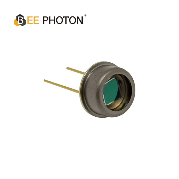
Si-PIN-Photodiode mit niedrigem Dunkelstrom (350-1060nm) PDCC14-001
Unsere Si-PIN für die Präzisionsphotometrie bietet außergewöhnliche Genauigkeit für empfindliche Lichtmessungen. Mit ihrem niedrigen Dunkelstrom ist diese Fotodiode ideal für analytische und wissenschaftliche Instrumente, die präzise Ergebnisse erfordern.
Die große Debatte: Photovoltaik-Modus vs. Photoleitungs-Modus
Lassen Sie uns kurz kontrovers werden. Die Branche ist besessen vom Photoleitungs-Modus (Anlegen einer Sperrspannung). Ja, das Anlegen einer Sperrspannung verbreitert die Sperrschicht, senkt die Sperrschichtkapazität und macht die Diode extrem schnell. Großartig für Glasfaser und Telekommunikation.
Aber für medizinische Präzisionsmessungen? Das ist meistens eine schlechte Idee.
Wenn Sie eine Sperrvorspannung anlegen, erzeugen Sie einen konstanten Dunkelstrom. Dieser Dunkelstrom verursacht Schrotrauschen. Das Schrotrauschen ist proportional zum Gleichstrom, der durch das Bauteil fließt. Wenn Sie versuchen, ein schwaches Fluoreszenzsignal einer Blutprobe zu detektieren, wird dieses Schrotrauschen Ihr Signal vollständig überlagern.
Stattdessen verwenden wir den Photovoltaik-Modus (unvorgespannt, 0 V). In diesem Modus ist der Dunkelstrom praktisch gleich null. Der Photostrom variiert linear zum einfallenden Licht, und die Temperaturstabilität ist wesentlich besser. Aber was verursacht das Rauschen ohne Dunkelstrom?
Sie haben es erraten. Der Photodioden-Parallelwiderstand.
Im Photovoltaik-Modus wird das thermische Rauschen des Nebenschlusswiderstand zum absolut dominierenden Stromrauschen im System. Wenn Sie an Ihrem Detektor sparen und einen mit niedrigem Rsh kaufen, verschlechtern Sie Ihr SNR (Signal-Rausch-Verhältnis) massiv, noch bevor das Signal überhaupt den Verstärker erreicht.
Die Mathematik des Rauschens (ohne akademischen Jargon)
Ich habe versprochen, praxisnah zu bleiben, aber wir müssen uns die eigentliche Mathematik ansehen, um die Nachteile eines schlechten Rsh zu verstehen. Keine Sorge, ich werde keine unleserliche Formatierung verwenden.
Das thermische Rauschen (oft auch Johnson-Rauschen genannt), das durch den Nebenschlusswiderstand erzeugt wird, ist ein Stromrauschen. Sie können es mit dieser Standardformel berechnen:
Ij = √( 4 * k * T * B / Rsh )
Betrachten wir die einzelnen Teile dieses Puzzles:
- Ij ist der thermische Rauschstrom (in Amps RMS).
- k ist die Boltzmann-Konstante (1,38 x 10^-23 J/K).
- T ist die absolute Temperatur in Kelvin (die Zimmertemperatur liegt bei etwa 298 K).
- B ist Ihre Rauschmessbandbreite in Hz.
- Rsh ist der Photodioden-Parallelwiderstand in Ohm.
Sehen Sie sich an, wo Rsh sitzt in dieser Formel. Er befindet sich im Nenner.
Wenn Ihr Nebenschlusswiderstand steigt, sinkt Ihr thermischer Rauschstrom. Es handelt sich um eine inverse Quadratwurzelbeziehung. Wenn Sie Ihr Detektorrauschen halbieren möchten, benötigen Sie eine Fotodiode mit dem vierfachen Nebenschlusswiderstand.
Deshalb können Sie bei der Messung von extrem niedrigen Lichtstärken, etwa in einem Impulsdetektor oder einem Analysespektrometer, keine Fotodiode mit einem Rsh von 10 MΩ akzeptieren. Sie benötigen hunderte Megaohm oder vorzugsweise Gigaohm.
Die Operationsverstärker-Falle: Wie der Parallelwiderstand Verstärker ruiniert
Hier ist der Punkt, über den fast jeder Nachwuchsingenieur, mit dem ich je gearbeitet habe, stolpert. Die Fotodiode existiert nicht im luftleeren Raum. Man schließt sie an einen Transimpedanzverstärker (TIA) an, um diesen winzigen Fotostrom in eine nutzbare Spannung umzuwandeln.
Ein Standard-TIA verfügt über einen Operationsverstärker und einen Rückkopplungswiderstand (Rf). Wenn Sie winzige Signale messen, wird Ihr Rf massiv sein – vielleicht 100 MΩ oder sogar 1 GΩ, nur um eine ausreichende Verstärkung zu erzielen.
Aber Operationsverstärker sind nicht perfekt. Sie haben ihr eigenes internes Eingangsspannungsrauschen. Und wie viel von diesem OP-Spannungsrauschen erscheint an Ihrem Ausgang? Das hängt von der Rauschverstärkung der Schaltung ab.
Für niedrige Frequenzen wird die Rauschverstärkung (NG) eines TIA wie folgt angenähert:
Rauschverstärkung = 1 + ( Rf / Rsh )
Erkennen Sie die Falle?
Wenn Sie eine preiswerte Fotodiode mit einem Nebenschlusswiderstand von 5 MΩ verwenden und für Ihr Signal einen Rückkopplungswiderstand von 500 MΩ benötigen, beträgt Ihre Rauschverstärkung:
1 + (500 / 5) = 101.
Ihre Schaltung nimmt das Eigenrauschen der Spannung Ihres teuren, “rauscharmen” Operationsverstärkers und multipliziert es mit 101! Ihr Ausgang wird auf dem Oszilloskop wie eine flauschige Raupe aussehen.
Stellen Sie sich nun vor, Sie hätten einen Premium-Detektor von einem spezialisierten Hersteller für kundenspezifische Fotodioden wie BeePhoton bezogen. Sie setzen eine Diode ein mit einem Rsh von 2 GΩ.
Ihre neue Rauschverstärkung beträgt:
1 + (500 / 2000) = 1.25.
Sie haben Ihre Spannungsrauschverstärkung um fast das 100-fache reduziert, nur indem Sie einen Detektor mit einem angemessenen Photodioden-Parallelwiderstand. gewählt haben. Dies ist das Erfolgsgeheimnis beim Design medizinischer Geräte.

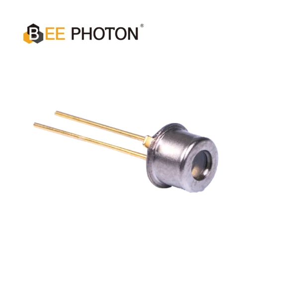
Si-PIN-Photodiode mit niedrigem Dunkelstrom (350-1060nm) PDCD10-001
Erzielen Sie genaue Ergebnisse mit unserer Wide Spectral Response Photodiode. Diese Si-PIN-Photodiode (350-1060 nm) zeichnet sich durch eine außergewöhnliche Empfindlichkeit und einen niedrigen Dunkelstrom aus, was sie perfekt für analytische Instrumente macht. Ihr harzbeschichtetes DIP-Gehäuse gewährleistet Langlebigkeit für alle Ihre Anforderungen in der Spektralphotometrie und bei analytischen Messungen.
Temperaturabhängigkeit: Die “6er-Regel”
Sie haben Ihre Schaltung also auf Ihrem Labortisch bei 22 °C getestet und alles sieht bestens aus. Dann kommt Ihr Gerät in eine Krankenhausumgebung, steht neben einem warmen Netzteil, die Temperatur im Gehäuseinneren erreicht 35 °C, und plötzlich schlägt die Kalibrierung der Maschine fehl. Was ist passiert?
Shunt-Widerstand ist stark temperaturabhängig. Er verharrt nicht einfach in einem Zustand. Mit steigender Temperatur nimmt der Diffusionsstrom zu, und Ihr Nebenschlusswiderstand fällt rapide ab.
Die Faustregel der Branche lautet wie folgt: Shunt-Widerstand halbiert sich in etwa bei jedem Temperaturanstieg um 6 °C. (Umgekehrt verdoppelt er sich bei jeder Senkung um 6 °C).
Wenn man bei 20 °C mit einem Rsh von 500 MΩ beginnt:
- Bei 26 °C sinkt er auf 250 MΩ.
- Bei 32 °C sinkt er auf 125 MΩ.
- Bei 38 °C liegt er nur noch bei 62,5 MΩ.
Das thermische Rauschen nimmt schleichend zu, und die TIA-Rauschverstärkung explodiert, da der Nenner (Rsh) schrumpft. Genau aus diesem Grund benötigen Medizinprodukte ein intensives Wärmemanagement oder – noch besser – Detektoren, die mit einem so astronomisch hohen Nebenschlusswiderstand beginnen, dass sie selbst nach einer thermischen Leistungsminderung noch einwandfrei funktionieren.
Materialfragen: Silizium vs. InGaAs vs. Germanium
Nicht alle Halbleiter sind gleich. Das gewählte Material begrenzt grundlegend den/die Nebenschlusswiderstand den/die Sie erreichen können.
Wenn Sie im sichtbaren bis nahen Infrarotspektrum arbeiten (z. B. 400 nm bis 1100 nm), ist Silizium (Si) unangefochten. Die Bandlücke von Silizium ermöglicht außergewöhnlich hohe Rsh-Werte, weshalb Si-PIN-Photodioden die Standardwahl für die medizinische Bildgebung und die Biowissenschaften sind.
Sobald man in den Bereich längerer Infrarotwellenlängen vordringt, müssen Materialien mit kleineren Bandlücken wie InGaAs oder Germanium verwendet werden. Eine kleinere Bandlücke bedeutet mehr thermisch erzeugte Ladungsträger bei Raumtemperatur, was den/die drastisch senkt. Nebenschlusswiderstand.
Hier ist eine kurze Referenztabelle, die ich auf der Grundlage typischer Werte bei Raumtemperatur zusammengestellt habe. (Bedenken Sie, dass auch die Größe der aktiven Fläche diese Zahlen beeinflusst – größere aktive Flächen weisen einen niedrigeren Rsh auf).
| Photodiodenmaterial | Typischer Parallelwiderstand (Rsh) | Hauptanwendung | Rauschprofil im PV-Modus |
|---|---|---|---|
| Silizium (Si-PIN) | 100 MΩ bis > 5 GΩ | Medizintechnik (CT), Pulsoximetrie, Spektroskopie | Hervorragend / Extrem niedrig |
| InGaAs | 1 MΩ bis 50 MΩ | Telekommunikation, NIR-Spektroskopie | Mäßig |
| Germanium (Ge) | 1 kΩ bis 100 kΩ | Ältere IR-Detektion, Leistungsmesser | Mangelhaft / Hohes Rauschen |
Wie Sie sehen, sollten Sie bei der Entwicklung lebensrettender Geräte auf Silizium setzen, wann immer die Wellenlänge dies zulässt.
Praxis-Fallstudie: Rettung eines IVD-Fluoreszenz-Lesegeräts
Ich möchte eine anonymisierte Geschichte eines Kunden teilen, mit dem wir vor Kurzem zusammengearbeitet haben. Dieser entwickelte ein In-vitro-Diagnostik (IVD)-Fluoreszenz-Lesegerät. Das Konzept war brillant, aber der Prototyp scheiterte kläglich. Das Fluoreszenzsignal ihrer Assays war so unglaublich schwach, dass es im Grundrauschen ihrer Detektorplatine völlig unterging.
Ihr leitender Ingenieur rief mich an, sichtlich aufgelöst. “Der Operationsverstärker rauscht”, sagte er. “Wir brauchen einen besseren Operationsverstärker.”
Ich bat darum, ihren Schaltplan zu sehen. Sie verwendeten einen erstklassigen Operationsverstärker in Elektrometer-Qualität. Der Operationsverstärker war nicht das Problem.
Dann sah ich mir das Datenblatt der generischen Standard-Fotodiode an, die sie bei einem großen Katalogdistributor gekauft hatten. Das garantierte Minimum Photodioden-Parallelwiderstand war mit nur 10 MΩ angegeben.
Da sie eine enorme Verstärkung benötigten, um die Fluoreszenz zu erkennen, betrug ihr Rückkopplungswiderstand 2 GΩ.
Ihr Rauschgewinn betrug 1 + (2000 / 10) = 201.
Das Grundrauschen des Operationsverstärkers wurde um das 201-fache verstärkt! Zudem überlagerte der thermische Rauschstrom eines 10-MΩ-Widerstands bei Raumtemperatur die tatsächlichen Photonen, die auf das Silizium trafen.
Ich sagte ihnen, sie sollten die generische Diode ausbauen. Wir ersetzten sie durch einen unserer spezialisierten Detektoren, indem wir sie dazu anregten, unsere Si-PIN-Fotodiodes. Das spezifische Modell, das wir ihnen lieferten, war spezialpassiviert, um einen Nebenschlusswiderstand von über 3 Gigaohm zu garantieren.
Die mathematische Grundlage änderte sich schlagartig.
Neue Rauschverstärkung: 1 + (2000 / 3000) = 1,66.
Das Grundrauschen sank um Größenordnungen. Plötzlich konnten sie Fluoreszenzkonzentrationen messen, die 50-mal niedriger waren als ihre bisherige Nachweisgrenze. In der darauffolgenden Woche bestanden sie ihre interne Validierung.
Das passiert, wenn man die physikalischen Gesetze der Nebenschlusswiderstand.
Si-PIN-Photodiode mit niedrigem Dunkelstrom (350-1060nm) PDCT14-001
Verbessern Sie Ihre optischen Messgeräte mit unserer Si-PIN-Photodiode im TO-Gehäuse. Sie zeichnet sich durch einen extrem niedrigen Dunkelstrom, hohe Konsistenz und ein Borosilikatfenster für lange Haltbarkeit aus. Diese Hochleistungs-Si-PIN-Photodiode ist für anspruchsvolle Anwendungen optimiert.
Wie wir den Parallelwiderstand im Labor tatsächlich messen
Sie fragen sich vielleicht: “Woher weiß ich, ob das Datenblatt lügt?”
Ehrlich gesagt ist der einzige Weg, sicherzugehen, die eigene Messung. Aber man kann nicht einfach ein Standard-Multimeter an die Diodenanschlüsse halten. Die Ausgangsspannung eines Standard-DMMs würde die Diode zu stark in Durchlass- oder Sperrrichtung vorspannen und so den zu messenden Widerstand komplett verfälschen.
Shunt-Widerstand ist streng auf 0 V definiert. Um ihn experimentell zu bestimmen, muss eine winzige Spannung angelegt werden – typischerweise exakt +10 mV und anschließend -10 mV.
Man legt +10 mV an, misst den Strom mit einem ultrapräzisen Picoamperemeter (wie einem Keithley-Elektrometer) und berechnet R = U / I. Dasselbe wiederholt man bei -10 mV, um die Symmetrie zu gewährleisten und den Durchschnitt zu bilden.
Da die Ströme im Picoampere-Bereich liegen, würden jegliches Umgebungsrauschen, Vibrationen (Mikrofonie) oder Streulicht die Messung verfälschen. Die Diode muss sich in absoluter Dunkelheit befinden, thermisch stabilisiert sein und in einem faradayschen Käfig platziert werden.
Wenn Sie nicht über die entsprechende Ausrüstung verfügen, müssen Sie sich auf einen Anbieter verlassen, der seine Dioden tatsächlich testet, anstatt nur theoretische Werte anzugeben.
Ein Wort zur aktiven Fläche
Es gibt einen Kompromiss, den ich erwähnen muss. Man kann nicht einfach 10 GΩ Nebenschlusswiderstand für einen Detektor von der Größe eines Speisetellers verlangen.
Shunt-Widerstand ist umgekehrt proportional zur aktiven Fläche der Fotodiode. Wenn Sie die Fläche des Siliziumchips verdoppeln, verdoppeln Sie das Volumen, in dem thermische Ladungsträgergeneration stattfinden kann. Ihr Nebenschlusswiderstand halbiert sich.
Das bedeutet, dass mechanisches und optisches Design Hand in Hand mit dem elektronischen Rauschen gehen. Wenn Sie eine Linse verwenden können, um das Licht auf eine kleinere Fotodiode zu fokussieren, können Sie eine Diode mit einer kleineren aktiven Fläche einsetzen. Eine kleinere aktive Fläche bedeutet einen höheren Nebenschlusswiderstand, eine geringere Sperrschichtkapazität und ein massiv verbessertes Signal-Rausch-Verhältnis.
Hören Sie auf, 10x10mm Detektoren zu verwenden, wenn ein 3x3mm Detektor mit einer günstigen Kunststofflinse Ihnen 10-mal weniger Rauschen liefert!
Warum Qualitätsfertigung wichtig ist
Die Herstellung einer Fotodiode mit einem außergewöhnlich hohen Nebenschlusswiderstand geht nicht nur darum, gute Silizium-Wafer zu kaufen. Es kommt ganz auf den Fertigungsprozess an.
An den Rändern des P-N-Übergangs zerstört der Leckstrom den Rsh. Wenn die Passivierungsschicht (die Oxidschicht, die das rohe Silizium schützt) schlecht gewachsen ist oder wenn während des Diffusionsprozesses Verunreinigungen eingebracht werden, entsteht Oberflächenleckage. Die Oberflächenleckage wirkt wie ein parasitärer Widerstand parallel zu Ihrer Diode und lässt Ihren gesamten Nebenschlusswiderstand.
Wenn Sie Ihre Bauteile von einem spezialisierten Hersteller für kundenspezifische Fotodioden wie BeePhoton, beziehen, erhalten Sie Silizium, das mit einer unglaublich strengen Kontrolle der Übergangspassivierung und des Getterings verarbeitet wurde. So bringen wir unsere Photodioden-Parallelwiderstand in den Giga-Ohm-Bereich, in dem generische Marken einfach nicht mithalten können.
Si-PIN-Photodiode mit niedrigem Dunkelstrom (350-1060nm) PDCT01-201
Erleben Sie überragende Signalklarheit mit unserer Si-PIN-Photodiode, die für extrem niedrigen Dunkelstrom und hohe Stabilität entwickelt wurde. Diese Fotodiode gewährleistet eine präzise Lasererkennung und optische Messungen. Unsere Si-PIN-Photodiode mit niedrigem Dunkelstrom bietet außergewöhnliche Leistung.
Häufig gestellte Fragen (FAQ)
1. Kann ich den Nebenschlusswiderstand meiner Fotodiode erhöhen?
Sie können den intrinsischen Wert Nebenschlusswiderstand des physischen Diodenchips nach seiner Herstellung nicht mehr erhöhen, aber Sie können seine Leistung in Ihrem Gerät durch Senkung der Temperatur maximieren. Da dieser Nebenschlusswiderstand sich etwa alle 6 °C Temperaturabsenkung verdoppelt, wird der Einsatz eines thermoelektrischen Kühlers (TEC) zur Kühlung der Fotodiode den Rsh-Wert drastisch erhöhen und Ihr thermisches Rauschen verringern.
2. Spielt der Parallelwiderstand eine Rolle, wenn ich eine Sperrvorspannung (Photoleitungsmodus) verwende?
Nicht wirklich. Wenn Sie eine Sperrvorspannung von 5 V oder 10 V anlegen, wechselt die dominierende Rauschquelle vom thermischen Rauschen des Nebenschlusswiderstand zum Schrotrauschen des Dunkelstroms. Wenn Ihre Anwendung für hohe Geschwindigkeiten ausgelegt ist und Sie die Diode vorspannen, sollten Sie Ihre Aufmerksamkeit stattdessen auf die Minimierung des Dunkelstroms und der Sperrschichtkapazität richten. Rsh ist ausschließlich ein kritischer Parameter für den Betrieb ohne Vorspannung (Photovoltaik-Betrieb).
3. Warum schwingt meine TIA-Schaltung, obwohl mein Shunt-Widerstand hoch ist?
Während ein hoher Photodioden-Parallelwiderstand löst Probleme mit der Spannungsrauschverstärkung, behebt jedoch keine Kapazitätsprobleme. Wenn Ihre Schaltung oszilliert, liegt das wahrscheinlich daran, dass die Sperrschichtkapazität der Fotodiode mit dem Rückkopplungswiderstand Ihres Operationsverstärkers interagiert und einen Pol in der Rückkopplungsschleife erzeugt. Sie müssen einen kleinen Rückkopplungskondensator (Cf) parallel zu Ihrem Rückkopplungswiderstand hinzufügen, um den Verstärker zu stabilisieren.
4. Was ist ein “guter” Shunt-Widerstandswert für medizinische Geräte?
Für präzise medizinische Anwendungen wie die Pulsoximetrie oder das CT-Scanning unter Verwendung eines Siliziumdetektors mit einer aktiven Fläche von etwa 5 mm² sollten Sie einen Nebenschlusswiderstand von mindestens 250 MΩ bis 1 GΩ bei Raumtemperatur fordern. Wenn Ihr Datenblatt 10 MΩ angibt, suchen Sie sich einen besseren Detektor.
Lassen Sie uns Ihre Rauschprobleme gemeinsam lösen
Die Navigation durch die Physik des rauscharmen Analogdesigns ist schwierig, und Sie sollten nicht raten müssen, ob Ihr Detektor in der Praxis funktioniert oder versagt. Wenn Sie mit einem schlechten Signal-Rausch-Verhältnis (SNR), übermäßigem thermischen Rauschen oder der Spannungsrauschverstärkung des Operationsverstärkers zu kämpfen haben, könnte das Problem einfach an dem Stück Silizium liegen, das Sie verwenden.
Lassen Sie nicht länger zu, dass schlechte Nebenschlusswiderstand Ihre präzisen medizinischen Designs ruinieren. Wir sind darauf spezialisiert, Detektoren zu entwickeln, die an die absoluten Grenzen der rauscharmen Zero-Bias-Performance gehen.
Bereit für ein Upgrade Ihrer Schaltung? Besuchen Sie unsere Kontaktseite, um mit unserem Engineering-Team in Kontakt zu treten, oder senden Sie direkt eine Nachricht an info@photo-detector.com. Erzählen Sie uns von Ihrem Grundrauschen, und weisen Ihnen genau nach, wie ein geeigneter kundenspezifischer Detektor dies beheben kann.