La cruda realidad sobre el diseño para polarización cero
Mire, diseñar equipos de medición de precisión ya es bastante difícil sin que el ruido del detector arruine el proceso. Si está construyendo un oxímetro de pulso de alta gama, un escáner de TC de rayos X o un lector de diagnóstico in vitro, probablemente ya sepa que la polarización cero es el camino a seguir.
Pero aquí está el detalle que nadie explica realmente en las clases estándar de electrónica: el verdadero héroe (o villano absoluto) de su circuito es la resistencia de derivación del fotodiodo.
Veo a diseñadores todo el tiempo aplicando una polarización inversa masiva a sus diodos porque creen que necesitan “velocidad”. Alerta de spoiler: para aplicaciones médicas de baja frecuencia y poca luz, probablemente no sea así. Aplicar una polarización inversa solo inyecta un molesto ruido de disparo y corriente oscura en un sistema que no puede permitírselo. Usted quiere operar en modo fotovoltaico. Y en modo fotovoltaico, resistencia shunt dicta casi todo sobre su umbral de ruido.
La mayoría de los fabricantes genéricos de detectores le venden basura en lo que respecta al rendimiento real con polarización cero. Citan una especificación “típica” en la página cuatro de una hoja de datos, pero cuando realmente lo conecta a su amplificador de transimpedancia, su relación señal-ruido se echa a perder por completo.
Analicemos qué resistencia shunt es en realidad, por qué determina el éxito o el fracaso de un circuito médico de precisión y cómo puede evitar que su amplificador operacional amplifique ruido puro.
¿Qué es realmente la resistencia shunt (Rsh) de un fotodiodo?
Si observa el circuito equivalente de un fotodiodo, no es solo una pequeña fuente de corriente perfecta. Tiene una fuente de corriente en paralelo con una capacitancia de unión (Cj) y una resistencia. Esa resistencia en paralelo es su resistencia shunt (generalmente escrita como Rsh).
¿En palabras sencillas? Es la resistencia de la unión del fotodiodo con polarización cero. Si observa la curva de corriente-voltaje (I-V) de un fotodiodo, la resistencia shunt es literalmente la pendiente de la curva justo en el origen, donde V = 0.
En un universo perfectamente ideal y físicamente imposible, un fotodiodo tendría una resistencia shunt. infinita. Sin fugas, sin problemas. En el mundo real, los valores actuales varían desde decenas de ohmios (para algunos materiales infrarrojos realmente deficientes o específicos) hasta miles de megaohmios (gigaohmios) para silicio de alta calidad.
¿Por qué los diseñadores de equipos médicos se preocupan tanto por este único parámetro? Porque cuando se opera a 0 V (modo fotovoltaico), no se tiene corriente oscura proveniente de una polarización aplicada. La fuente dominante de ruido en su detector es el ruido térmico generado por esa exacta resistencia shunt . Si su Rsh es baja, su ruido es alto. Es lo que hay. A la termodinámica no le importan los plazos de entrega de su proyecto.

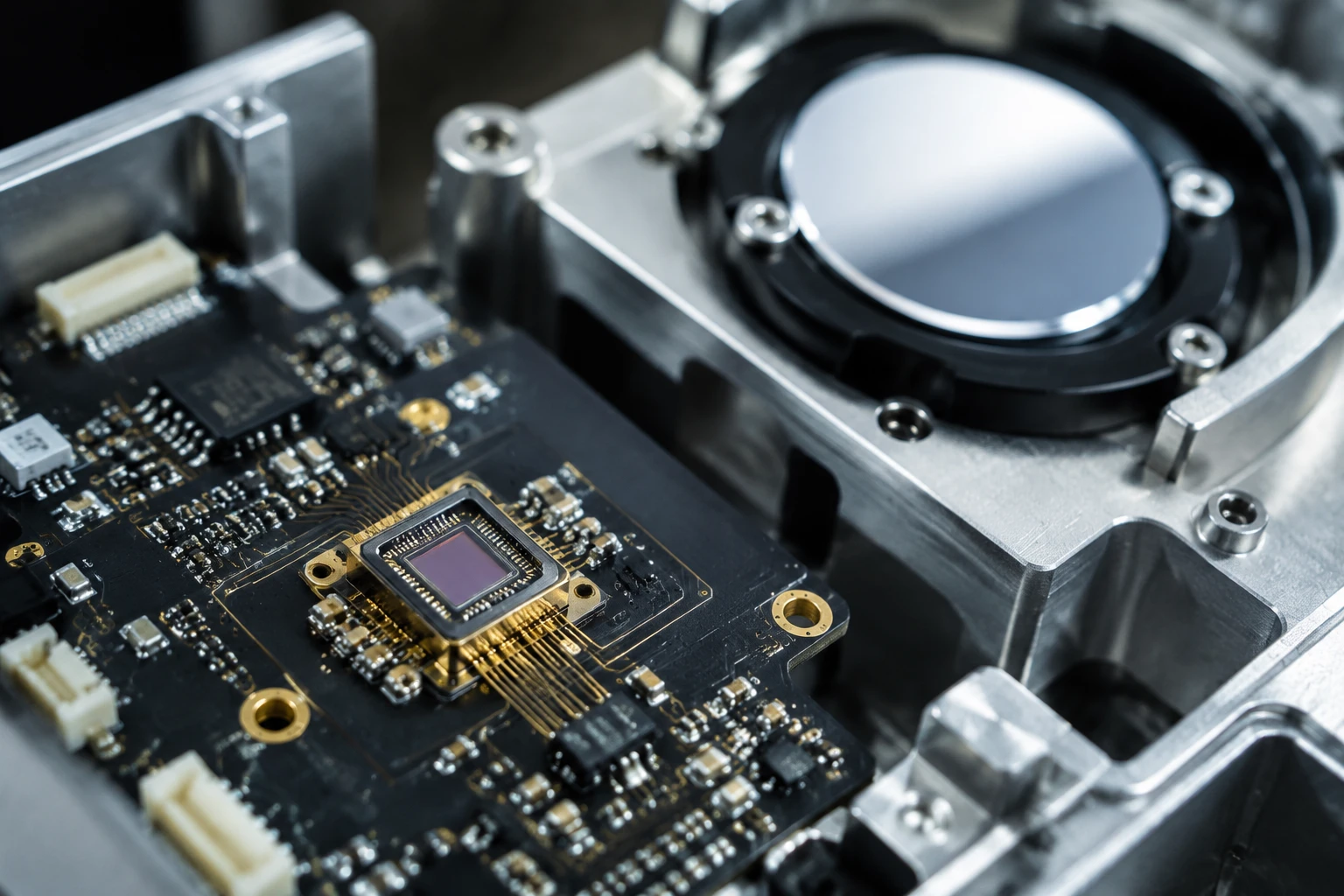
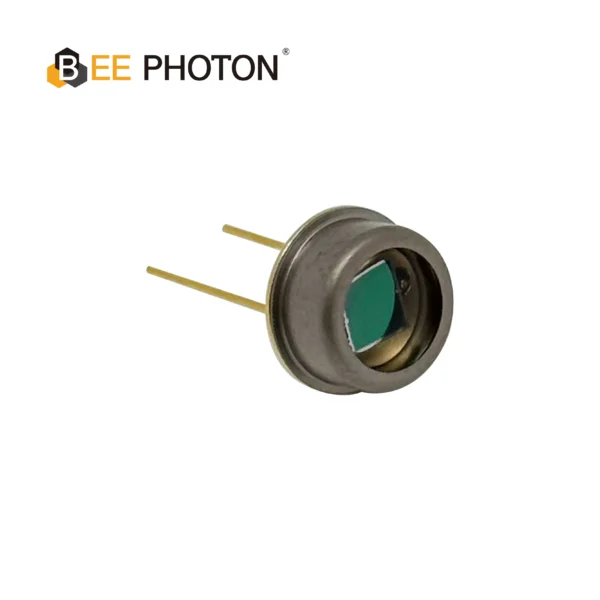
Fotodiodo PIN de Si con baja corriente oscura (350-1060nm) PDCC14-001
Nuestro PIN de Si para fotometría de precisión ofrece una exactitud excepcional para la medición de luz sensible. Con baja corriente oscura, este fotodiodo es ideal para instrumentos analíticos y científicos que requieren resultados precisos.
El gran debate: modo fotovoltaico frente a modo fotoconductivo
Pongámonos polémicos por un segundo. La industria está obsesionada con el modo fotoconductivo (aplicar una polarización inversa). Sí, la polarización inversa ensancha la región de agotamiento, reduce la capacitancia de la unión y hace que el diodo sea súper rápido. Excelente para fibra óptica y telecomunicaciones.
¿Pero para mediciones médicas de precisión? Por lo general, es una idea terrible.
Cuando se aplica una polarización inversa, se crea una corriente oscura constante. Esa corriente oscura genera ruido de disparo. El ruido de disparo es proporcional a la corriente continua (CC) que fluye a través del dispositivo. Si se intenta detectar una señal de fluorescencia débil de una muestra de sangre, ese ruido de disparo ocultará su señal por completo.
En su lugar, utilizamos el modo fotovoltaico (sin polarización, 0 V). En este modo, la corriente oscura es esencialmente cero. La fotocorriente varía linealmente con la luz incidente y la estabilidad de la temperatura es mucho mejor. Pero sin corriente oscura, ¿qué causa el ruido?
Lo ha adivinado. El resistencia de derivación del fotodiodo.
En el modo fotovoltaico, el ruido térmico de la resistencia shunt se convierte en el ruido de corriente absolutamente dominante en el sistema. Si escatima en su detector y compra uno con una Rsh baja, estará perjudicando su SNR (relación señal-ruido) incluso antes de que la señal llegue al amplificador.
La matemática del ruido (sin la jerga académica)
Prometí que esto sería práctico, pero debemos observar las matemáticas reales para comprender el problema de una Rsh deficiente. No se preocupe, no utilizaré formatos ilegibles.
El ruido térmico (a menudo llamado ruido de Johnson) generado por la resistencia shunt es un ruido de corriente. Puede calcularlo utilizando esta fórmula estándar:
Ij = √( 4 * k * T * B / Rsh )
Veamos las piezas de este rompecabezas:
- Ij es la corriente de ruido térmico (en amperios RMS).
- k es la constante de Boltzmann (1,38 x 10^-23 J/K).
- T es la temperatura absoluta en Kelvin (la temperatura ambiente es de aproximadamente 298 K).
- B es el ancho de banda de la medición de ruido en Hz.
- Rsh es la resistencia de derivación del fotodiodo en ohmios.
Observe dónde Rsh se encuentra en esa fórmula. Está en el denominador.
Si su resistencia shunt aumenta, la corriente de ruido térmico disminuye. Es una relación de raíz cuadrada inversa. Si desea reducir el ruido de su detector a la mitad, necesita un fotodiodo con cuatro veces la resistencia shunt.
Es por esto que, cuando se miden niveles de luz ultra bajos en algo como un detector de pulsos o un espectrómetro analítico, no se puede aceptar un fotodiodo con una Rsh de 10 MΩ. Se necesitan cientos de megaohmios, o preferiblemente gigaohmios.
La trampa del amplificador operacional: Cómo la resistencia de derivación arruina los amplificadores
Aquí está la parte que afecta a casi todos los ingenieros principiantes con los que he trabajado. El fotodiodo no existe en el vacío. Se conecta a un amplificador de transimpedancia (TIA) para convertir esa pequeña fotocorriente en un voltaje utilizable.
Un TIA estándar tiene un amplificador operacional y una resistencia de retroalimentación (Rf). Si está midiendo señales diminutas, su Rf va a ser masiva, tal vez 100 MΩ o incluso 1 GΩ, solo para obtener suficiente ganancia.
Pero los amplificadores operacionales no son perfectos. Tienen su propio ruido de voltaje de entrada interno. ¿Y cuánto de ese ruido de voltaje del amplificador operacional aparece en su salida? Depende de la ganancia de ruido del circuito.
Para bajas frecuencias, la ganancia de ruido (NG) de un TIA se aproxima por:
Ganancia de Ruido = 1 + ( Rf / Rsh )
¿Ve la trampa?
Si utiliza un fotodiodo económico con una resistencia shunt de 5 MΩ, y necesita una resistencia de retroalimentación de 500 MΩ para su señal, su ganancia de ruido es:
1 + (500 / 5) = 101.
¡Su circuito está tomando el ruido de voltaje innato de su costoso amplificador operacional de “bajo ruido” y multiplicándolo por 101! Su salida se verá como una oruga peluda en el osciloscopio.
Ahora, imagine que adquirió un detector premium de un fabricante especializado en fotodiodos personalizados como BeePhoton. Instala un diodo con una Rsh de 2 GΩ.
Su nueva ganancia de ruido es:
1 + (500 / 2000) = 1.25.
Acaba de reducir la amplificación del ruido de voltaje casi 100 veces simplemente eligiendo un detector con una adecuada resistencia de derivación del fotodiodo. Este es el ingrediente secreto del diseño de equipos médicos.

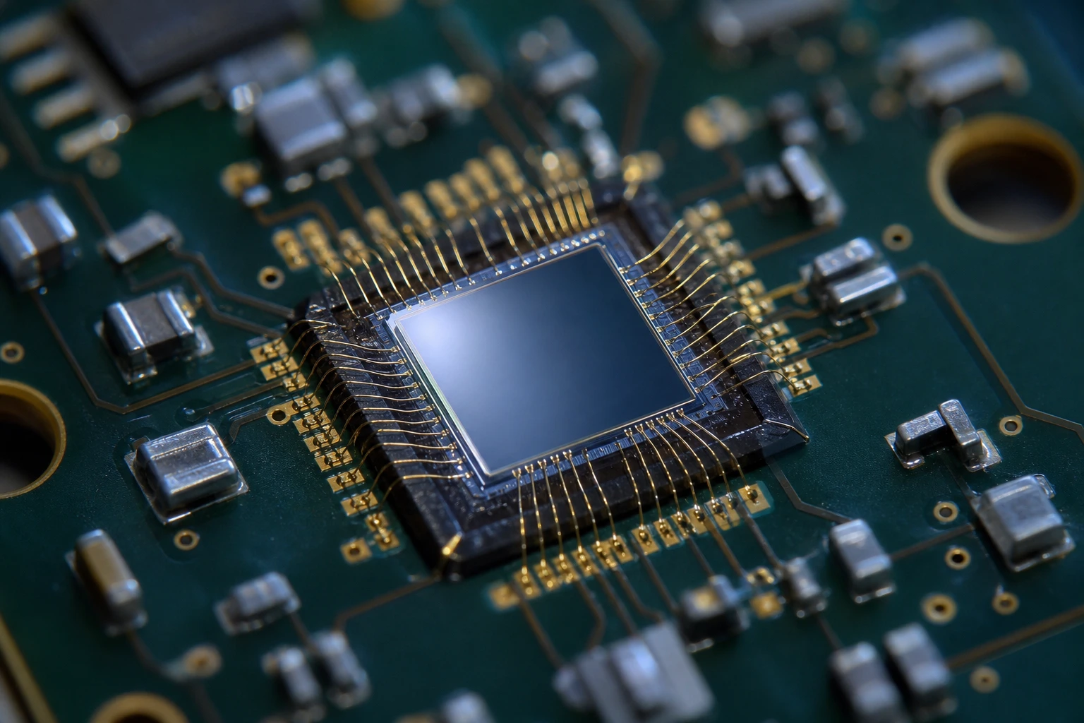
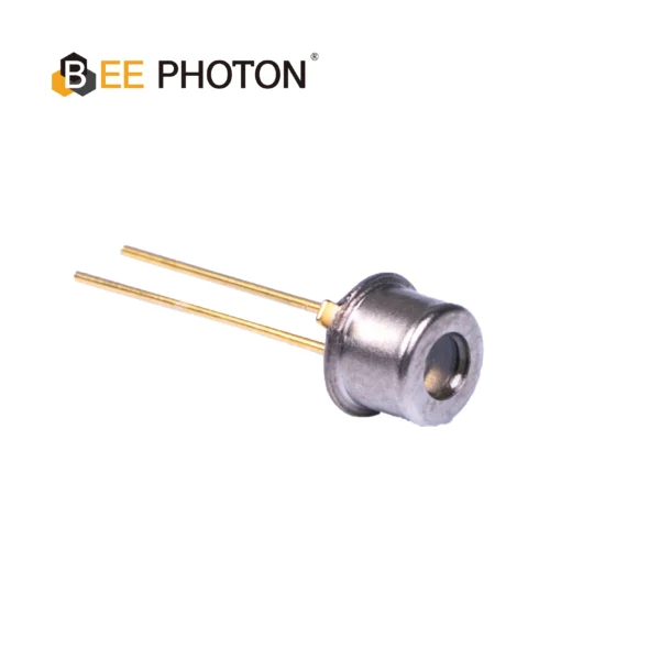
Fotodiodo PIN de Si con baja corriente oscura (350-1060nm) PDCD10-001
Consiga resultados precisos con nuestro fotodiodo de respuesta espectral amplia. Este fotodiodo PIN de Si (350-1060 nm) presenta una sensibilidad excepcional y una corriente oscura baja, perfecta para instrumentos analíticos. Su encapsulado DIP recubierto de resina garantiza la durabilidad para todas sus necesidades de espectrofotometría y medición analítica.
Dependencia de la temperatura: La “Regla del 6”
Así que probó su circuito en su banco de laboratorio a 22°C y todo parece ir genial. Luego, su dispositivo va a un entorno hospitalario, se coloca junto a una fuente de alimentación caliente, la temperatura interna de la carcasa alcanza los 35°C y, de repente, la máquina falla en la calibración. ¿Qué pasó?
Resistencia de derivación depende en gran medida de la temperatura. No permanece estática. A medida que la temperatura sube, la corriente de difusión aumenta, y su resistencia shunt cae en picado.
La regla empírica de la industria es la siguiente: Resistencia de derivación se reduce aproximadamente a la mitad por cada aumento de 6 °C en la temperatura. (Por el contrario, se duplica por cada disminución de 6 °C).
Si se comienza con una Rsh de 500 MΩ a 20 °C:
- A 26 °C, cae a 250 MΩ.
- A 32 °C, cae a 125 MΩ.
- A 38 °C, baja a 62,5 MΩ.
El ruido térmico aumenta paulatinamente y la ganancia de ruido del TIA se dispara porque el denominador (Rsh) disminuye. Esta es exactamente la razón por la que los dispositivos médicos requieren una gestión térmica intensiva o, mejor aún, detectores que comiencen con una cifra tan astronómicamente alta de resistencia shunt que incluso tras una degradación térmica, sigan funcionando a la perfección.
La importancia del material: Silicio frente a InGaAs frente a Germanio
No todos los semiconductores son iguales. El material elegido limita fundamentalmente la resistencia shunt que se puede alcanzar.
Si se trabaja en el espectro visible al infrarrojo cercano (como de 400 nm a 1100 nm), el silicio (Si) es el rey. La banda prohibida (bandgap) del silicio permite valores de Rsh excepcionalmente altos, razón por la cual los fotodiodos PIN de Si son la elección predeterminada para la imagen médica y las ciencias de la vida.
Al pasar a longitudes de onda infrarrojas más largas, es necesario utilizar materiales con bandas prohibidas más pequeñas, como el InGaAs o el germanio. Una banda prohibida menor implica más portadores generados térmicamente a temperatura ambiente, lo que reduce drásticamente la resistencia shunt.
A continuación se presenta una tabla de referencia rápida basada en valores típicos a temperatura ambiente. (Tenga en cuenta que el tamaño del área activa también modifica estas cifras: las áreas activas más grandes tienen una Rsh menor).
| Material del fotodiodo | Resistencia shunt típica (Rsh) | Aplicación principal | Perfil de ruido en modo PV |
|---|---|---|---|
| Silicio (Si PIN) | 100 MΩ a > 5 GΩ | Tomografía computarizada médica, oximetría de pulso, espectroscopía | Excelente / Extremadamente bajo |
| InGaAs | 1 MΩ a 50 MΩ | Telecomunicaciones, espectroscopía NIR | Moderado |
| Germanio (Ge) | 1 kΩ a 100 kΩ | Detección IR antigua, medidores de potencia | Deficiente / Ruido alto |
Como puede ver, si está diseñando equipos para salvar vidas, preferirá el silicio siempre que la longitud de onda lo permita.
Estudio de caso del mundo real: Rescatando un lector de fluorescencia IVD
Quiero compartir una historia anónima de un cliente con el que trabajamos recientemente. Estaban diseñando un lector de fluorescencia para diagnóstico in vitro (IVD). El concepto era brillante, pero su prototipo estaba fallando estrepitosamente. La señal de fluorescencia de sus ensayos era tan increíblemente débil que se perdía por completo en el ruido de fondo de su placa detectora.
Su ingeniero principal me llamó, prácticamente entrando en pánico. “El amplificador operacional hace ruido”, dijo. “Necesitamos un amplificador operacional mejor”.”
Pedí ver su esquema. Estaban usando un amplificador operacional de grado electrómetro de primer nivel. El amplificador operacional no era el problema.
Luego miré la hoja de datos del fotodiodo genérico de serie que compraron a un gran distribuidor de catálogo. El mínimo garantizado resistencia de derivación del fotodiodo estaba listado como solo 10 MΩ.
Debido a que necesitaban una ganancia masiva para ver la fluorescencia, su resistencia de retroalimentación era de 2 GΩ.
Su ganancia de ruido era 1 + (2000 / 10) = 201.
¡El ruido de fondo del amplificador operacional se estaba amplificando 201 veces! Además, la corriente de ruido térmico de una resistencia de 10 MΩ a temperatura ambiente estaba ahogando los fotones reales que golpeaban el silicio.
Les dije que desecharan el diodo genérico. Lo reemplazamos con uno de nuestros detectores especializados invitándoles a explorar nuestro Fotodiodo PIN de Sis. El modelo específico que les proporcionamos fue pasivado de forma personalizada para garantizar una resistencia shunt de más de 3 gigaohmios.
Los cálculos cambiaron instantáneamente.
Nueva ganancia de ruido: 1 + (2000 / 3000) = 1.66.
El ruido de base disminuyó en órdenes de magnitud. De repente, pudieron leer concentraciones de fluorescencia 50 veces inferiores a su límite de detección anterior. Superaron su validación interna la semana siguiente.
Esto es lo que sucede cuando se respeta la física de la resistencia shunt.
Fotodiodo PIN de Si con baja corriente oscura (350-1060nm) PDCT14-001
Mejore su equipo de medición óptica con nuestro fotodiodo PIN de Si con embalaje TO. Presenta una corriente oscura ultrabaja, alta consistencia y una ventana de borosilicato para una mayor durabilidad. Este fotodiodo PIN de Si de alto rendimiento está optimizado para aplicaciones exigentes.
Cómo medimos realmente la resistencia en derivación en el laboratorio
Quizás se esté preguntando: “¿Cómo sé si la hoja de datos me está mintiendo?”
Sinceramente, la única forma de estar seguro es medirla usted mismo. Pero no basta con conectar un multímetro estándar a los pines del diodo. La salida de voltaje de un DMM estándar polarizará el diodo en directo o en inverso en exceso, alterando por completo la resistencia que se intenta medir.
Resistencia de derivación se define estrictamente a 0 V. Para medirla experimentalmente, hay que aplicar un voltaje minúsculo; normalmente, exactamente +10 mV y luego -10 mV.
Se aplican +10 mV, se utiliza un picoamperímetro de ultraprecisión (como un electrómetro Keithley) para medir la corriente y se calcula R = V / I. Luego se hace lo mismo a -10 mV para asegurar la simetría y promediar los resultados.
Debido a que las corrientes están en el rango de los picoamperios, cualquier ruido ambiental, vibración (microfonía) o luz parásita arruinará la medición. El diodo debe estar en absoluta oscuridad, estabilizado térmicamente y dentro de una jaula de Faraday.
Si no dispone del equipo para hacerlo, debe confiar en un proveedor que realmente pruebe sus diodos en lugar de limitarse a imprimir números teóricos.
Unas palabras sobre el área activa
Hay un compromiso técnico que debo mencionar. No se puede exigir simplemente 10 GΩ resistencia shunt en un detector del tamaño de un plato de comida.
Resistencia de derivación es inversamente proporcional al área activa del fotodiodo. Si se duplica el área del chip de silicio, se está duplicando el volumen donde puede ocurrir la generación térmica de portadores. Su resistencia shunt se reduce a la mitad.
Esto significa que el diseño mecánico y el diseño óptico van de la mano con el ruido electrónico. Si puede utilizar una lente para enfocar la luz en un fotodiodo más pequeño, podrá usar un diodo con un área activa menor. Un área activa más pequeña significa una mayor resistencia shunt, una menor capacitancia de unión y una relación señal-ruido enormemente mejorada.
¡Deje de usar detectores de 10x10 mm cuando un detector de 3x3 mm con una lente de plástico económica le proporcionará 10 veces menos ruido!
¿Por qué es importante la fabricación de calidad?
Crear un fotodiodo con un nivel excepcionalmente alto de resistencia shunt no se trata solo de comprar obleas de silicio de buena calidad. Depende totalmente del proceso de fabricación.
Los bordes de la unión P-N son donde la corriente de fuga destruye la Rsh. Si la capa de pasivación (el recubrimiento de óxido que protege el silicio en bruto) se desarrolla de forma deficiente, o si se introducen impurezas durante el proceso de difusión, se producen fugas superficiales. La fuga superficial actúa como una resistencia parásita en paralelo con su diodo, hundiendo su total de resistencia shunt.
Cuando usted se abastece de un fabricante dedicado a fotodiodos personalizados como BeePhoton, usted obtiene silicio que ha sido procesado con un control increíblemente estricto sobre la pasivación de la unión y el proceso de gettering. Así es como llevamos nuestra resistencia de derivación del fotodiodo al territorio de los gigaohmios, donde las marcas genéricas simplemente no pueden competir.
Fotodiodo PIN de Si con baja corriente oscura (350-1060nm) PDCT01-201
Experimente una claridad de señal superior con nuestro fotodiodo PIN de Si, diseñado para una corriente oscura ultrabaja y una gran estabilidad. Este fotodiodo garantiza una detección láser y unas mediciones ópticas precisas. Nuestro fotodiodo Si PIN de baja corriente oscura ofrece un rendimiento excepcional.
Preguntas más frecuentes (FAQ)
1. ¿Puedo aumentar la resistencia de derivación de mi fotodiodo?
No se puede aumentar la resistencia shunt del chip físico del diodo una vez fabricado, pero puede maximizar su rendimiento en su dispositivo reduciendo la temperatura. Porque resistencia shunt duplica aproximadamente cada 6°C de descenso de la temperatura, el uso de un refrigerador termoeléctrico (TEC) para enfriar el fotodiodo aumentará drásticamente el Rsh y reducirá su ruido térmico.
2. ¿Importa la resistencia de derivación si utilizo una polarización inversa (modo fotoconductor)?
La verdad es que no. Cuando se aplica una polarización inversa de 5V o 10V, la fuente de ruido dominante pasa del ruido térmico del resistencia shunt al ruido de disparo de la corriente oscura. Si su aplicación es de alta velocidad y está polarizando el diodo, debería centrar su atención en minimizar la corriente oscura y la capacitancia de unión. Rsh es estrictamente un parámetro crítico para el funcionamiento con polarización cero (fotovoltaico).
3. ¿Por qué mi circuito TIA oscila a pesar de que mi resistencia de derivación es alta?
Mientras que un alto resistencia de derivación del fotodiodo resuelve problemas de ganancia de ruido de voltaje, pero no soluciona problemas de capacitancia. Si su circuito está oscilando, es probable que la capacitancia de unión del fotodiodo esté interactuando con la resistencia de retroalimentación de su amplificador operacional para crear un polo en el lazo de retroalimentación. Debe agregar un pequeño condensador de retroalimentación (Cf) en paralelo con su resistencia de retroalimentación para estabilizar el amplificador.
4. ¿Cuál es un “buen” valor de resistencia shunt para equipos médicos?
Para aplicaciones médicas de precisión, como la pulsioximetría o la tomografía computarizada, que utilizan un detector de silicio con un área activa de unos 5 mm², se debe exigir un resistencia shunt de al menos 250 MΩ a 1 GΩ a temperatura ambiente. Si su hoja de datos dice 10 MΩ, busque un detector mejor.
Solucionemos sus problemas de ruido juntos
Navegar por la física del diseño analógico de bajo ruido es difícil, y usted no debería tener que adivinar si su detector funcionará o fallará en el campo. Si tiene problemas con una relación señal-ruido (SNR) deficiente, ruido térmico excesivo o amplificación de ruido de voltaje del amplificador operacional, el problema podría ser simplemente el trozo de silicio que está utilizando.
Deje de permitir que una mala resistencia shunt arruine sus diseños médicos de precisión. Nos especializamos en la ingeniería de detectores que superan los límites absolutos del rendimiento de bajo ruido y polarización cero.
¿Listo para mejorar su circuito? Diríjase a nuestra página de contacto para ponerse en contacto con nuestro equipo de ingeniería, o simplemente envíe un mensaje directamente a info@photo-detector.com. Cuéntenos sobre su umbral de ruido y le mostraremos exactamente cómo un detector personalizado adecuado puede solucionarlo.