If you are a system architect or an optical design engineer, you have probably spent some sleepless nights staring at your Bill of Materials (BOM). You are staring at that one line item—the photodetector—and asking yourself if you really need to spend top dollar on Indium Gallium Arsenide (InGaAs), or if you can get away with cheap, reliable Silicon (Si).
This design headache gets real when you are working in the 900 nm to 1100 nm wavelength band, especially for galvanometer-based scanning systems (Galvo systems). Whether it is a high-speed laser marking machine, a LiDAR setup, or a 3D metal printing system, your choice of a near infrared PIN photodiode chip is what keeps your beam positioning precise and your signal-to-noise ratio (SNR) clean.
Let’s skip the textbook fluff and look at the actual physics, the real-world trade-offs, and how to choose the right near infrared PIN photodiode chip for your Galvo system without blowing your project budget.
Why the 900nm to 1100nm Band is an Engineering Battleground
Before we talk about the sensors themselves, we need to talk about why this specific wavelength range is so popular yet so difficult.
The 900-1100 nm band is home to some of the most common lasers in the world. You have Nd:YAG and Ytterbium fiber lasers operating at 1064 nm. You have GaAs semiconductor lasers shooting out 905 nm and 940 nm beams. These wavelengths are awesome because they can pass through common optical fibers easily, they have decent atmospheric transmission, and they match the emission spectrum of many industrial processes.
But here is the catch: this band lies right on the boundary of where Silicon stops working and InGaAs starts shining.
For a silicon-based near infrared PIN photodiode chip, 1100 nm is the absolute end of the road. It represents the physical limit of the material’s bandgap. For an InGaAs-based near infrared PIN photodiode chip, this range is on the lower end of its sweet spot. This overlap means both materials are technically options, but they behave very differently in practice. If you choose the wrong near infrared PIN photodiode chip, you might end up with a system that is either way too expensive or plagued by terrible signal drift.
The Core Physics: Bandgaps and Responsivity (Without the Math Nightmare)
Let’s look at why these two materials behave the way they do. It all comes down to the bandgap energy of the semiconductor material inside your near infrared PIN photodiode chip.
Silicon (Si) has a bandgap of about 1.12 electron-volts (eV) at room temperature.
Indium Gallium Arsenide (InGaAs), specifically the type lattice-matched to Indium Phosphide, has a much smaller bandgap of around 0.75 eV.
To generate an electrical signal, an incoming photon must have enough energy to kick an electron across this bandgap. The relationship between the cutoff wavelength (expressed as lambda_c) and the bandgap energy (Eg) can be written as:
lambda_c = 1240 / Eg
Where lambda_c is in nanometers (nm) and Eg is in eV.
If we run the numbers for a silicon-based near infrared PIN photodiode chip, we get:
lambda_c = 1240 / 1.12 = 1107 nm
This is why a silicon near infrared PIN photodiode chip goes completely blind beyond 1100 nm. As you approach this limit, the photons simply do not have enough energy to excite the electrons. They pass right through the silicon crystal like it is window glass.
For a standard InGaAs near infrared PIN photodiode chip, the calculation gives us:
lambda_c = 1240 / 0.75 = 1653 nm
This means an InGaAs near infrared PIN photodiode chip can easily absorb photons all the way up to 1650 nm, making the 900-1100 nm band a walk in the park for this material.
Looking at how absorption changes across this band highlights the main differences:
From 900 nm to 950 nm, Silicon maintains high quantum efficiency, making it highly competitive.
From 950 nm to 1000 nm, Silicon’s absorption begins dropping steadily, requiring larger active areas or better amplification.
At 1064 nm, Silicon’s performance is poor, making it highly transparent, whereas InGaAs maintains high, stable quantum efficiency across the entire 900 nm to 1100 nm range.
Quantum Efficiency and Responsivity
Quantum efficiency (QE) is the percentage of incident photons that successfully create electron-hole pairs inside your near infrared PIN photodiode chip. Responsivity (R) is the actual current output you get per watt of incident light, measured in Amps per Watt (A/W).
The relationship between the two is simple:
R = (QE * q * lambda) / (h * c)
Or, in simpler terms:
R is approximately equal to (QE * lambda) / 1240
At 940 nm, a high-quality silicon near infrared PIN photodiode chip like the chip de fotodiodo PIN PDC-C2928-NIR-B de 940 nm can achieve a QE of over 70%, resulting in a responsivity of about 0.55 A/W.
But watch what happens when we move to 1064 nm. The QE of standard silicon drops off a cliff, often falling below 15%. This leaves you with a tiny responsivity of around 0.12 A/W.
In contrast, an InGaAs near infrared PIN photodiode chip maintains a QE of nearly 90% across the entire 900-1100 nm range. At 1064 nm, its responsivity sits comfortably at 0.78 A/W. That is a massive difference in signal strength.
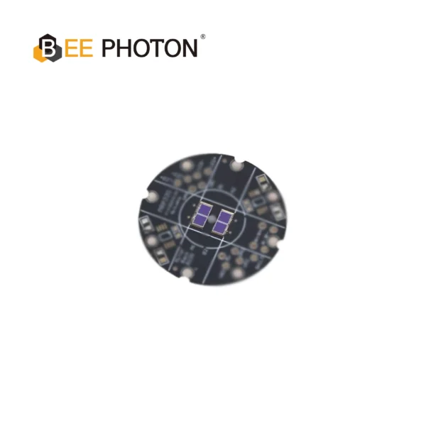
Fotodiodos PIN de Si para Galvo PDC-C2928-NIR-B
Optimice el escaneo con nuestro chip fotodiodo PIN de 940 nm, PDC-C2928-NIR-B. Este chip fotodiodo PIN de 940 nm garantiza una detección precisa de la posición del galvanómetro y un bajo nivel de ruido.
What Galvo Systems Actually Need from a Detector
A galvanometer system is essentially a pair of motor-driven mirrors that steer a laser beam very fast and very precisely. To keep those mirrors in check, the system needs real-time feedback.
Usually, a small fraction of the laser beam is split off and directed onto a near infrared PIN photodiode chip, or a separate tracking laser is bounced off the back of the mirrors onto the sensor.
To make this feedback loop work, your near infrared PIN photodiode chip must excel in three areas:
1. Speed (Rise Time and Bandwidth)
If your mirrors are moving at kilohertz speeds, your detector cannot be lagging behind. The rise time (tr) of your near infrared PIN photodiode chip limits the system’s response speed.
Rise time is mostly determined by the junction capacitance (Cj) of the near infrared PIN photodiode chip and the load resistance (RL) of your amplifier circuit:
tr is approximately equal to 2.2 * R * C
If you want a fast response, you need a near infrared PIN photodiode chip with low capacitance. This is tricky because large active areas—which are great for catching stray light from moving mirrors—naturally have higher capacitance.
2. Active Area and Position Sensing
A single-pixel detector is fine for monitoring absolute laser power. But for tracking mirror position, you often need a multi-segment near infrared PIN photodiode chip, like a bi-cell or a quad-cell.
When the beam shifts, the relative current from each segment of the near infrared PIN photodiode chip changes, telling your control loop exactly where the mirror is pointing.
If you choose a segmented near infrared PIN photodiode chip, the alignment of the segments must be extremely tight. Silicon fabrication technology is highly mature, allowing us to build a near infrared PIN photodiode chip with tiny gap widths between segments (often under 10 microns) at a low cost. Making a similar segmented near infrared PIN photodiode chip out of InGaAs is much more complex and incredibly expensive.
3. Noise and Dynamic Range
Industrial environments are noisy. You have power supplies, motors, and ambient light trying to mess up your signal.
To detect subtle changes in beam position, your near infrared PIN photodiode chip needs a low Noise Equivalent Power (NEP). NEP is the minimum optical power required to get a signal-to-noise ratio of 1.
A major contributor to noise is the dark current (Id)—the current that flows through the near infrared PIN photodiode chip even when it is pitch black. Silicon naturally has a much lower dark current at room temperature than InGaAs because of its wider bandgap. This means that at shorter wavelengths (like 900-940 nm), a silicon near infrared PIN photodiode chip can actually provide a cleaner signal than its InGaAs counterpart.
Comparing Silicon vs InGaAs Across Key Wavelengths
Let’s break down how these two materials handle the specific wavelengths you are likely working with.
The 905nm and 940nm Region: Silicon Dominates
If your Galvo system operates at 905 nm or 940 nm, the decision is easy.
A silicon-based near infrared PIN photodiode chip is highly sensitive in this range. Because silicon wafers are cheap to manufacture, you can get a relatively large active area for a fraction of what you would pay for InGaAs.
For instance, our chip de fotodiodo PIN PDC-C2928-NIR-B de 940 nm is a specialized silicon near infrared PIN photodiode chip designed specifically for high-performance 940 nm detection. It offers an optimized intrinsic layer thickness to maximize near-infrared absorption while keeping capacitance low enough for fast response times.
Another stellar choice for slightly shorter wavelengths is our fotodiodo PIN de silicio PDC-C2929, which works beautifully around 920 nm as an alternative near infrared PIN photodiode chip.
At these wavelengths, using an InGaAs near infrared PIN photodiode chip is usually overkill. You are paying a premium for sensitivity you do not need, and you might actually end up with higher dark current noise.
The 1064nm Region: The Tough Choice
This is where project meetings get heated.
At 1064 nm, a standard silicon near infrared PIN photodiode chip is on its deathbed. Its responsivity is very low, making it difficult to detect weak signals. If your Galvo system relies on picking up weak reflections or backscatter from a 1064 nm laser, a standard silicon near infrared PIN photodiode chip will struggle to get a good signal-to-noise ratio.
In contrast, an InGaAs near infrared PIN photodiode chip is a beast at 1064 nm. It has over five times the responsivity of standard silicon, giving you a strong, clear signal without needing massive amplification.
So, why doesn’t everyone just use InGaAs at 1064 nm?
Because of the BOM cost. An InGaAs near infrared PIN photodiode chip can easily cost 10 to 20 times more than a silicon chip of the same active area. If you are building a high-volume commercial product, that cost difference can make or break your margins.
The Temperature Problem
There is another hidden gotcha at 1064 nm: temperature.
Because 1064 nm is so close to the bandgap limit of silicon, the absorption coefficient of silicon at this wavelength is highly sensitive to temperature changes. As a silicon near infrared PIN photodiode chip warms up (either from the ambient environment or from absorbing high-power laser energy), its bandgap narrows slightly.
This narrow shift actually increases its responsivity at 1064 nm. While more signal sounds good, a drifting responsivity is a nightmare for precise feedback calibration. Your system will literally drift out of alignment as the machine heats up.
An InGaAs near infrared PIN photodiode chip, on the other hand, is operating far from its bandgap limit at 1064 nm. Its temperature coefficient of sensitivity is extremely low and highly stable. If your industrial Galvo system needs to run for hours in a hot factory without losing calibration, an InGaAs near infrared PIN photodiode chip is the safer bet.
Detailed Silicon vs InGaAs Performance Matrix
Let’s look at the raw numbers. Here is how a typical silicon near infrared PIN photodiode chip stacks up against an InGaAs near infrared PIN photodiode chip in the 900-1100 nm range.
| Parámetro | Silicon (Si) PIN Photodiode | Fotodiodo PIN de InGaAs | Winning Material for Galvo (900-1100nm) |
|---|---|---|---|
| Gama espectral | 320 nm to 1100 nm | 800 nm to 1700 nm | InGaAs (broader NIR coverage) |
| Responsivity @ 940nm | ~0.55 A/W | ~0.65 A/W | Corbata (Si is more cost-effective) |
| Responsivity @ 1064nm | ~0.12 A/W (Standard) / ~0.3 A/W (Enhanced) | ~0.78 A/W | InGaAs (massive signal advantage) |
| Dark Current (Room Temp) | Very Low (<0.1 nA for small areas) | Moderate (0.5 to 5 nA) | Silicio (quieter at room temp) |
| Capacitancia de unión | Bajo | Bajo | Corbata (depends on active area size) |
| Temperature Stability @ 1064nm | Poor (drifts significantly with temp) | Excellent (highly stable) | InGaAs (crucial for industrial stability) |
| Segmented Chip Gaps | Very clean (down to <10 µm gaps) | Harder to fabricate cleanly | Silicio (better for position sensing) |
| Relative Cost (Per Area) | 1x (Highly affordable) | 10x to 30x (Expensive) | Silicio (major budget saver) |
How to Save Your BOM Cost: The Segmented Silicon Option
If you are designing a Galvo position sensor for a 1064 nm system, you usually need a segmented (bi-cell or quad-cell) detector.
Imagine putting a quad-cell InGaAs near infrared PIN photodiode chip into your system. Because InGaAs wafers are small and difficult to process, a segmented InGaAs near infrared PIN photodiode chip with a decent active area is going to cost a fortune.
Here is how smart system architects beat this problem: they use an NIR-enhanced, segmented silicon near infrared PIN photodiode chip and compensate for the lower responsivity in their electronics.
By choosing a high-quality segmented silicon near infrared PIN photodiode chip like the segmented PIN photodiode chip PDC-2C3432-NIR-B de BeePhoton, you get a precise multi-segment layout with a high-quality NIR-enhanced silicon structure.
Yes, the raw signal from the silicon near infrared PIN photodiode chip at 1064 nm is lower than InGaAs. But by pairing the PDC-2C3432-NIR-B with a high-gain, low-noise Transimpedance Amplifier (TIA), you can boost that signal back up. Since the silicon near infrared PIN photodiode chip naturally has a very low dark current, you can ramp up the amplifier gain without immediately drowning your signal in noise.
This approach allows you to achieve the high-speed feedback your Galvo system needs while slashing your photodetector BOM cost by up to 80%.
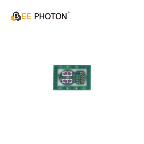
Fotodiodos PIN de Si para Galvo PDC-2C3432-NIR-B
En PDC-2C3432-NIR-B es un especializado chip de fotodiodo PIN segmentado diseñado para una retroalimentación de posición diferencial precisa en escáneres galvanométricos de alta velocidad. La integración de este canal dual chip de fotodiodo PIN segmentado permite que los sistemas obtengan un seguimiento angular preciso con un ruido de señal mínimo.
Real-World Case Studies from the Lab
Let’s look at two anonymous design scenarios we have helped our clients navigate over the last couple of years.
Case Study 1: The High-Speed 940nm LiDAR Tracking Loop
A design team was building a compact Galvo-driven LiDAR system for automated guided vehicles (AGVs) operating in warehouses. The laser wavelength was 940 nm.
The original prototype was built using an imported InGaAs detector because the designers assumed they needed the highest possible sensitivity for a “near-infrared” application. However, when trying to move the product to mass production, the unit cost of the InGaAs near infrared PIN photodiode chip was killing their margins.
Comparing the original high-cost design with the optimized low-cost design highlights the core changes:
In the original prototype, they used an InGaAs quad-cell photodiode costing approximately $120.00. This was paired with a standard TIA stage.
In the updated, optimized design, they switched to the BeePhoton PDC-C2928 silicon near infrared PIN photodiode chip costing approximately $4.50. To balance the performance, they paired it with an optimized low-noise TIA stage.
We sat down with them and looked at their optical path. At 940 nm, the quantum efficiency of our chip de fotodiodo PIN PDC-C2928-NIR-B de 940 nm silicon near infrared PIN photodiode chip is incredibly high.
They swapped the expensive InGaAs chip for our silicon PDC-C2928-NIR-B near infrared PIN photodiode chip. The result? They saved over $100 per unit on BOM costs.
Because silicon has a lower dark current at room temperature, their noise floor actually dropped, resulting in a cleaner signal and a slightly better overall tracking accuracy.
Case Study 2: The Industrial 1064nm Laser Marker
An industrial laser marking company was upgrading their Galvo feedback control loop for a 1064 nm fiber laser system. The Galvo mirrors were operating in a hot, uncooled industrial housing that regularly reached 55°C.
Initially, they tried to use a low-cost, standard silicon near infrared PIN photodiode chip. While it worked fine during morning calibration tests, the system began to drift after running for an hour. The laser marker would lose precision, ruining expensive metal parts.
The problem was thermal drift. At 55°C, the responsivity of their standard silicon near infrared PIN photodiode chip at 1064 nm had drifted by nearly 20% compared to its room-temperature performance.
To solve this, they had two choices:
First, they could pay a massive premium to switch to an InGaAs near infrared PIN photodiode chip.
Second, they could design a complex active cooling and thermal calibration circuit for the silicon near infrared PIN photodiode chip.
Because their production volume was relatively low but their precision requirements were absolute, they decided that switching to a high-reliability InGaAs near infrared PIN photodiode chip was the best path forward. The stable temperature coefficient of InGaAs completely resolved the calibration drift, proving that sometimes, paying for premium materials is the only way to meet demanding environmental specs.
Step-by-Step Selection Decision Tree
How do you decide which near infrared PIN photodiode chip is right for your project? Use this quick decision tree:
What is your laser wavelength?
If you are working with 900 nm to 950 nm (e.g., 905nm, 940nm), you should go with a Silicon near infrared PIN photodiode chip like the PDC-C2928-NIR-B o PDC-C2929. InGaAs is an unnecessary expense here.
If you are working at 1064 nm, you need to look at your budget and operating conditions.
What is your target BOM budget?
If you have a tight budget and high-volume production, use an NIR-enhanced Silicon near infrared PIN photodiode chip like the PDC-2C3432-NIR-B and invest some engineering time into a high-gain, low-noise TIA pre-amplifier circuit.
If you need high-end performance, low-volume, or are building a premium product, go with an InGaAs near infrared PIN photodiode chip to get maximum responsivity and thermal stability right out of the box.
How demanding is your operating temperature environment?
If your system operates in a stable room temperature environment (like lab instruments or indoor AGVs), a silicon near infrared PIN photodiode chip is highly viable, even at 1064 nm, provided your light levels are reasonable.
If your system faces wide temperature swings (like factory floors or outdoor LiDAR), an InGaAs near infrared PIN photodiode chip is highly recommended for 1064 nm systems to prevent thermal drift.
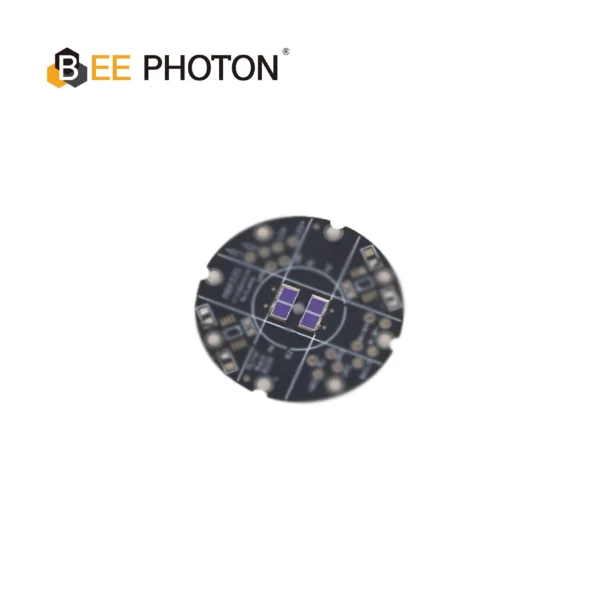
Fotodiodos PIN de Si para Galvo PDC-C2929
El PDC-C2929 es un chip de fotodiodo PIN de silicio de 920 nm económico. Este fotodiodo PIN de silicio de 920 nm ofrece un seguimiento estable y rentable de la posición del escáner.
FAQ: Clearing Up the Confusion
¿Puedo utilizar un chip de fotodiodo PIN de silicio para infrarrojo cercano para detectar un haz láser de 1064 nm?
Yes, you can, but it is not a simple drop-in solution. Because silicon’s responsivity at 1064 nm is low (usually between 0.1 and 0.25 A/W), you will get a much weaker electrical signal compared to using InGaAs. To make it work, you will need to design a high-performance pre-amplifier (like a transimpedance amplifier) and ensure your optical alignment is spot on to capture as many photons as possible with your near infrared PIN photodiode chip.
¿Por qué un chip de fotodiodo PIN de silicio para el infrarrojo cercano presenta tanta deriva a 1064 nm?
Silicon’s physical bandgap is roughly 1.12 eV, which corresponds to an absorption cutoff of about 1100 nm. Since 1064 nm is extremely close to this physical limit, even tiny changes in temperature will shift the silicon crystal’s bandgap slightly. When the temperature rises, the bandgap narrows, which dramatically increases the material’s ability to absorb 1064 nm photons. This causes the responsivity of your near infrared PIN photodiode chip to drift upward, throwing off your Galvo system’s calibration.
¿Es un chip de fotodiodo PIN de infrarrojo cercano de InGaAs siempre mejor que el de silicio?
No, definitivamente no. Si está operando en longitudes de onda inferiores a 950 nm, un chip fotodiodo PIN de silicio para infrarrojo cercano suele ser la opción superior. El silicio generalmente ofrece una corriente oscura mucho más baja a temperatura ambiente, lo que significa que se obtiene una señal de línea de base más limpia con menos ruido. Además, el silicio es mucho más económico y fácil de fabricar en diseños complejos de múltiples segmentos, los cuales son fundamentales para el posicionamiento Galvo de alta velocidad.
¿Cómo afecta la capacitancia de unión a la velocidad del bucle de retroalimentación de mi galvo?
La capacitancia de unión actúa como un pequeño condensador integrado en su detector. Cuando la luz incide en el chip, esta capacitancia debe cargarse y descargarse, lo cual requiere tiempo. Si la capacitancia de unión es demasiado alta, actúa como un filtro de paso bajo, ralentizando su chip de fotodiodo PIN de infrarrojo cercano y limitando el ancho de banda de su bucle de control Galvo. Para mantener la velocidad, se requiere un chip de fotodiodo PIN de infrarrojo cercano con un área activa pequeña o un espesor de capa intrínseca optimizado para minimizar la capacitancia.
¿Cómo afecta la corriente oscura al rango dinámico de mi chip de fotodiodo PIN de infrarrojo cercano?
Dark current is the leakage current that flows through your near infrared PIN photodiode chip when no light is present. It creates a baseline shot noise that limits the smallest optical signal you can detect. At room temperature, Silicon has a much lower dark current than InGaAs, giving it an advantage in low-light, low-noise systems operating below 950 nm. However, at 1064 nm, InGaAs’s massive advantage in responsivity easily overcomes its higher dark current.
Get Your Optical Design Right the First Time
Choosing the right near infrared PIN photodiode chip is a delicate dance between physics, environmental demands, and cold, hard cash.
Are you currently working on a high-speed Galvo system and trying to figure out if you can safely swap your expensive InGaAs sensors for high-performance silicon to save on BOM costs? Or do you need a highly precise, custom segmented layout for a new industrial laser project?
Don’t guess and risk a costly redesign down the road. Our engineering team at BeePhoton has spent years designing, testing, and manufacturing specialized near infrared PIN photodiode chip variations. We can help you look at your optical path, evaluate your noise requirements, and select the exact near infrared PIN photodiode chip that fits your budget and your performance specs.
Envíenos un mensaje a info@photo-detector.com o visite nuestro página de contacto to share your project requirements. Let’s work together to build a robust, cost-effective detection system that keeps your Galvo mirrors tracking perfectly.