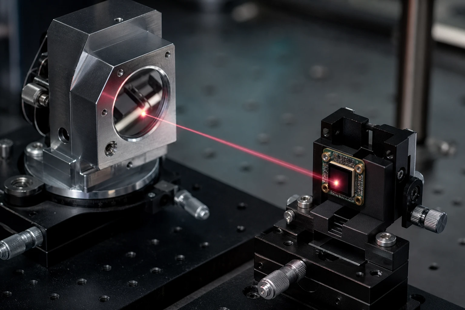
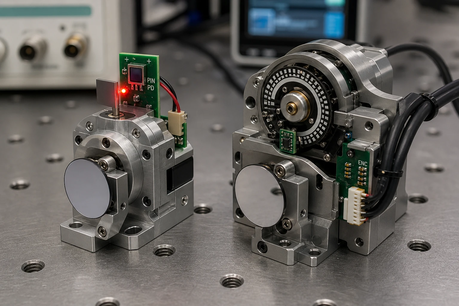
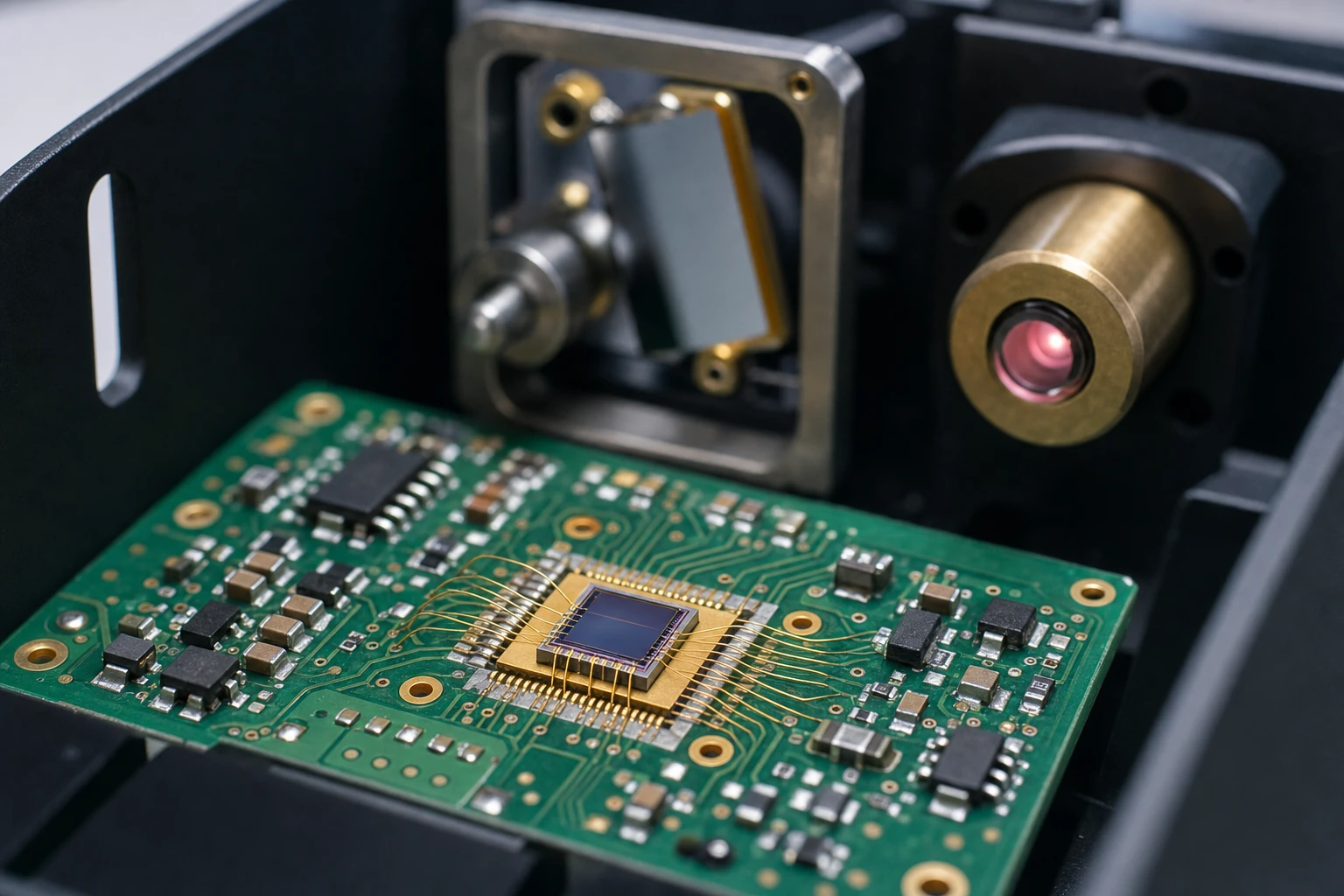
If you have spent hours on an optical bench trying to figure out why your galvo mirror position feedback starts getting wildly non-linear at the edges of your scan angle, you are not alone. Most structural optical engineers jump straight to blaming mirror inertia, driver amplifier tuning, or mechanical flexure. But more often than not, the real culprit is sitting right on the feedback board: a fundamental mismatch between your optical beam geometry and your photosensitive area active size photodiode specifications.
When designing high-speed optical scanning heads for laser marking, additive manufacturing, or medical imaging, getting the optical feedback loop right is everything. You need crisp response times, minimal phase lag, and rock-solid linear signal reproduction across the entire mechanical deflection range.
In this article, we are going to dive deep into how photodiode geometry impacts your galvo mirror tracking range. We will walk through the exact optical geometry math, examine real-world chip dimensions, evaluate spot size interaction, and look at actual engineering trade-offs so you can size your photodetector correctly on the first spin of your PCB design.
Photodiode Chip Dimension Outline vs. Active Photosensitive Area
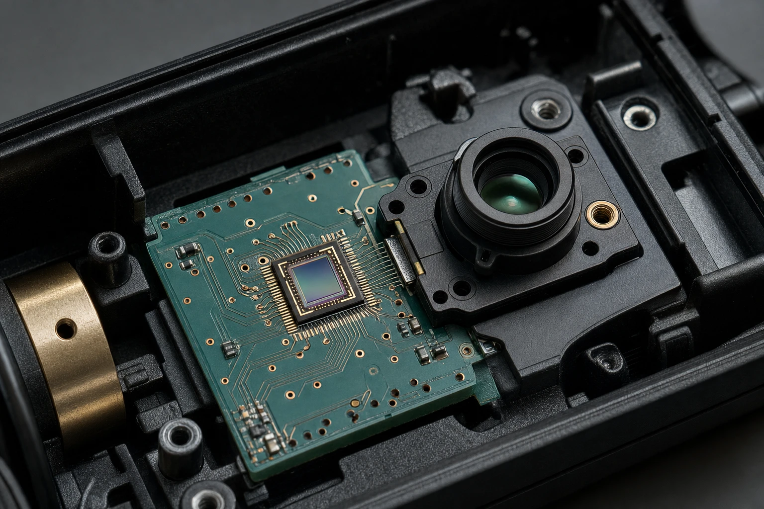
One of the most common mistakes in early-stage optomechanical packaging is confusing the physical die size with the light-sensitive surface area. When reading a detector datasheet, you will see two very distinct dimensional callouts: the photodiode chip dimension outline (the total physical footprint of the silicon die) and the actual active area dimensions.
The physical chip outline includes guard rings, passivation layer borders, bond pad real estate, and dicing street tolerances. The photosensitive active area, on the other hand, is strictly the p-n or p-i-n junction region exposed to incident photons where electron-hole pairs are efficiently collected to generate photocurrent.
Why does this matter so much for galvo tracking? Because your mechanical tolerance budget depends on total chip size for placement, but your optical tracking geometry cares exclusively about the active photosensitive boundary.
| Model / Sensor Category | Physical Chip Outline | Active Photosensitive Area | Junction Capacitance (VR = 5V) | Typical Galvo Tracking Setup |
|---|---|---|---|---|
| Single-Element PIN (Compact) | 3.2 x 3.2 mm | 2,9 x 2,9 mm | ~25 pF | Short-path high-speed feedback |
| Standard NIR Si PIN | 3.5 x 3.5 mm | 3.0 x 3.0 mm | ~30 pF | General industrial laser steering |
| Two-Element Segmented PIN | 3.4 x 3.2 mm | Dual (1.6 x 3.2 mm each) | ~18 pF per element | High-precision differential sensing |
When you specify a sensor like the PDC-C2928-NIR-B 940nm photodiode chip, you are looking at a tailored silicon layout designed to maximize active collection while keeping parasitical capacitance low enough for multi-kilohertz galvo feedback loops.
The Optical Geometry Math: Connecting Beam Deflection to Active Area
Let’s break down how a galvo mirror’s mechanical angle translates into physical spatial displacement across the photodetector face.
When a galvo mirror rotates by a mechanical angle Theta (measured in degrees or radians), the reflected optical beam deflects by twice that angle, or 2 * Theta. If the photodiode is positioned at an optical lever arm distance L from the center of rotation of the galvo mirror, the linear displacement Delta_X of the laser spot centroid across the photodiode plane is calculated as:
Delta_X = L * tan(2 * Theta)
For small angles, you can approximate this using the paraxial approximation:
Delta_X = 2 * L * Theta (where Theta is in radians)
However, the laser beam is not an infinitely small point source; it has a finite beam diameter or laser spot size photodetector footprint, typically defined at the 1/e^2 intensity threshold (d_s).
To maintain a linear response, the entire laser spot (or at least a fixed percentage of its energy distribution, such as 99%) must remain completely within the boundaries of the active photosensitive zone. Once the outer tail of the Gaussian beam profile spills over the edge of the active region—a phenomenon known as beam clipping—the photodiode output signal drops non-linearly relative to the mirror angle.
Therefore, the maximum unclipped linear beam displacement Delta_X_max allowed by your photosensitive area active size photodiode es:
Delta_X_max = (A_x – d_s) / 2
Dónde:
- A_x = Width of the active photosensitive area (for instance, 2.9 mm)
- d_s = Laser spot diameter at 1/e^2 on the photodiode face
Substituting this back into our mechanical angle equation gives us the maximum allowable mechanical tracking angle Theta_max:
Theta_max = 0.5 * arctan((A_x – d_s) / (2 * L))
Worked Engineering Example
Let’s run real numbers that structural optical engineers deal with every day on the bench.
- Active area dimension: square photodiode active area 2.9×2.9 mm (A_x = 2.9 mm)
- Incident laser spot diameter on detector: d_s = 0.8 mm
- Optical lever arm distance: L = 20 mm
First, calculate the maximum allowable spatial displacement:
Delta_X_max = (2.9 mm – 0.8 mm) / 2 = 1.05 mm
Now, solve for the maximum mechanical deflection angle of the galvo:
Theta_max = 0.5 * arctan(1.05 mm / 20 mm)
Theta_max = 0.5 * arctan(0.0525)
Theta_max = 0.5 * 3.005 degrees = 1.502 degrees (mechanical)
This translates to a total mechanical scan range of 3.004 degrees (or 6.008 degrees total optical sweep angle). If your application requires a mechanical scan angle of +/- 3.0 degrees, you immediately realize you have a problem: either your lever arm distance L must be reduced, your spot size d_s must be focused down, or you need a photosensitive area active size photodiode with larger active dimensions.
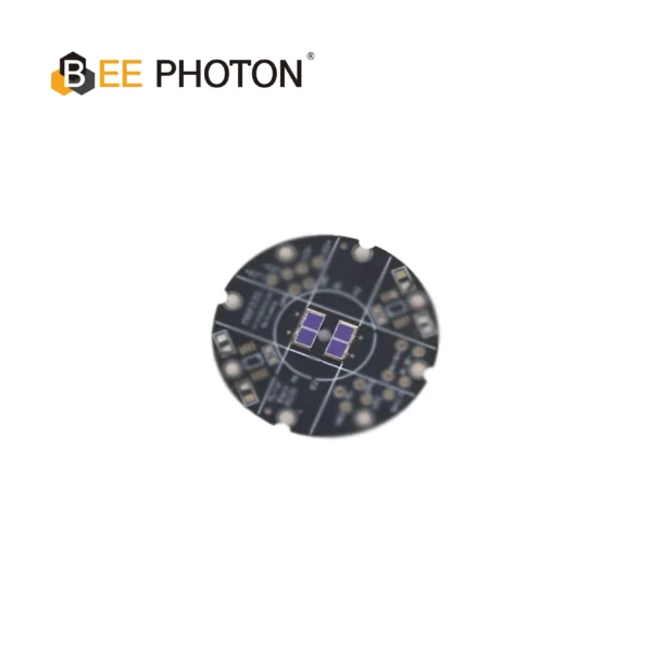
Fotodiodos PIN de Si para Galvo PDC-C2929
El PDC-C2929 es un chip de fotodiodo PIN de silicio de 920 nm económico. Este fotodiodo PIN de silicio de 920 nm ofrece un seguimiento estable y rentable de la posición del escáner.
How Photosensitive Area Size Shapes Galvo Tracking Limits
Elegir el correcto photosensitive area active size photodiode is always a game of compromises. You cannot simply drop in an enormous 10×10 mm photodiode chip and call it a day. In precision optical engineering, every parameter you tweak pulls another metric out of spec.
1. Junction Capacitance and Servo Bandwidth
The junction capacitance (C_j) of a silicon PIN photodiode is directly proportional to its active photosensitive area (A) and inversely proportional to the depletion layer width (w):
C_j = (Epsilon_r * Epsilon_0 * A) / w
If you double the active area to expand your tracking range, you double the capacitance. Higher capacitance introduces additional phase delay into your galvo control loop, lowering your phase margin and forcing you to roll off your servo bandwidth to prevent system oscillation.
When working with sensors like the fotodiodo PIN de silicio PDC-C2929, the active area is optimized specifically around 2.9×2.9 mm to hit a sweet spot: offering ample optical capture area while keeping junction capacitance down around ~25-30 pF at standard bias voltages.
2. Signal-to-Noise Ratio (SNR) and Dark Current
Dark current (I_d) also scales directly with active junction area. In position feedback systems operating at low optical power levels (to minimize thermal loading on the galvo structure), a larger active area brings higher shot noise and higher thermal noise (Johnson noise of the equivalent shunt resistance).
If your laser spot power drops below a critical irradiance threshold, noise on your photodiode output converts directly into position jitter in the galvo motor.
3. Spatial Responsivity Uniformity
Across a continuous silicon surface, responsivity is fairly uniform, but near the edges of the active area, localized electric field gradients can create a soft border zone. If your laser spot tracks too close to the perimeter of your photosensitive area active size photodiode, you will suffer from non-linear gain roll-off even before the geometric spot physically clips off the chip edge.
Differential Tracking with Segmented Photodiodes
For high-precision galvanometers, single-element photodiodes are often replaced by dual-element (bicell) or quadrant photodiodes. Instead of monitoring raw current amplitude, the system measures beam displacement by comparing the differential current between two adjacent active elements.
The position output signal S_pos is normalized as:
S_pos = (I_A – I_B) / (I_A + I_B)
When using a segmented photodiode such as the Diodo de fotodetección de PIN segmentado PDC-2C3432-NIR-B, the total tracking range depends on both the width of individual active elements and the narrow gap separating them (typically 10 to 50 micrometers).
Here, the linear tracking zone is governed by how far the center of the spot can move across the gap while maintaining overlap on both active halves:
Linear Tracking Displacement Limit = Spot Radius (d_s / 2)
If the laser spot moves so far to one side that it completely leaves Element A, I_A drops to zero, S_pos saturates at +1.0, and your feedback loop loses control. Thus, matching your spot size to the segmented photosensitive area active size photodiode layout is critical for ensuring smooth, continuous servo loop operation.
Real-World Engineering Case Study: Fixing Non-Linear Distortion in an Additive Scan Head
To see how these concepts play out on the bench, let’s review an actual engineering case study from an industrial client working on high-speed laser powder bed fusion (LPBF).
El problema
An optical engineering team was experiencing severe perimeter hatching errors on 3D printed metal parts. Their galvo scanning head worked flawlessly within a central +/- 5-degree field of view, but when steering beams toward the corners of the build plate (+/- 12 degrees), the galvo position encoder showed weird step-response overshoots and non-linear velocity ripple.
The original design used a custom optical pick-off mirror directing a 1.2 mm diameter 940nm laser pick-off spot onto a tiny photodiode with an active area of just 1.5 x 1.5 mm, placed 18 mm away from the galvo mirror axis.
Bench Diagnosis & Math
Plugging their setup into our deflection formula:
Delta_X_max = (1.5 mm – 1.2 mm) / 2 = 0.15 mm
Theta_max = 0.5 * arctan(0.15 mm / 18 mm) = 0.5 * arctan(0.00833) = 0.238 degrees
Their active tracking range was restricted to less than a quarter of a mechanical degree! Beyond that, over 80% of the laser spot energy was spilling off the detector edge. The transimpedance amplifier was starving for light, driving the gain into extreme non-linear clipping, which caused the galvo driver board to miscalculate mirror speed and overshoot positions.
La solución
The engineering team redesigned the pick-off block using a square photodiode active area 2.9×2.9 mm chip (PDC-C2928-NIR-B 940nm photodiode chip) and inserted a simple doublet lens to condense the feedback beam spot down from 1.2 mm to 0.5 mm at the sensor plane.
Let’s recalculate the new tracking margin:
Delta_X_max = (2.9 mm – 0.5 mm) / 2 = 1.20 mm
Theta_max = 0.5 * arctan(1.20 mm / 18 mm) = 0.5 * arctan(0.0667) = 1.908 degrees
By expanding the active area and focusing the spot size, the unclipped mechanical tracking range jumped by eight times (from 0.238 degrees to 1.908 degrees). The feedback signal linearity recovered immediately, eliminating the perimeter hatching defects on their 3D metal prints.
Mechanical Alignment Tolerances and Design Best Practices
When laying out your optomechanical assembly in CAD or optical modeling software, remember that your calculation for Theta_max represents the absolute ideal case. Real-world mechanical tolerances will quickly eat into your linear tracking margin.
Key Mechanical Variables to Account For:
- SMD Pick-and-Place Tolerance: Standard SMT placement processes can introduce +/- 0.05 mm to +/- 0.15 mm of translational position error on the PCB.
- PCB Mounting & Standoff Tolerances: Mechanical mounting holes on board assemblies usually carry +/- 0.1 mm clearance.
- Thermal Drift of Galvo Axis: As galvo drive coils heat up during long operating cycles, the zero-position center point can drift spatially by tens of micrometers.
- Wavelength Tilt: If your setup uses dual lasers (such as a 1064nm processing laser and a 635nm/920nm/940nm alignment beam), chromatic dispersion in pick-off optics can offset beam centers.
To keep your design reliable, we recommend applying a 30% Safety Buffer Margin to your active area geometry calculation:
A_effective = 0.70 * A_active
Theta_safe = 0.5 * arctan(( (0.70 * A_active) – d_s ) / (2 * L))
Engineering Trade-Off Matrix
| Design Objective | Primary Parameter Adjustment | Positive Impact | Potential Drawback / Risk |
|---|---|---|---|
| Expand Scan Range | Increase active area size | Broader angular coverage, easier assembly | Increased C_j, lower servo bandwidth |
| Increase Response Speed | Decrease active area size | Minimal phase lag, higher frequency capability | Tight optical alignment required, risk of beam clipping |
| Reduce Noise / Jitter | Shrink spot size on photodiode | Maximizes local power density, improves SNR | Demands extra focusing optics in pick-off path |
| Improve Tracking Accuracy | Use segmented photodiode | Superior differential position sensitivity | Gap loss between elements, requires dual TIA channels |
If you are working on custom optical setups or need specialized bare-die mounting layouts, you can explore specialized solution sets directly at BeePhoton high-performance photodetectors.
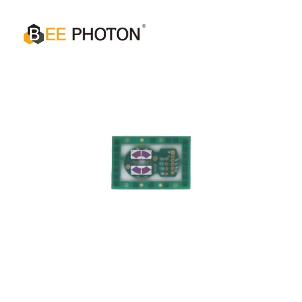
Fotodiodos PIN de Si para Galvo PDC-2C3432-NIR-B
En PDC-2C3432-NIR-B es un especializado chip de fotodiodo PIN segmentado diseñado para una retroalimentación de posición diferencial precisa en escáneres galvanométricos de alta velocidad. La integración de este canal dual chip de fotodiodo PIN segmentado permite que los sistemas obtengan un seguimiento angular preciso con un ruido de señal mínimo.
Preguntas más frecuentes (FAQ)
Q1: What is the main difference between photodiode chip dimension outline and active photosensitive area?
The photodiode chip dimension outline represents the total physical size of the silicon die (including dicing edges, anode/cathode wire bond pads, and perimeter guard rings). The active photosensitive area is the specific internal surface area designed to catch photons and generate photocurrent. For optical tracking calculations, you must always use the active photosensitive area size, not the overall physical die dimensions.
Q2: How does laser spot size affect my photodiode tracking linearity?
As long as the entire laser spot profile remains inside the active photosensitive boundary, the photodiode output scales linearly with total beam power. However, as soon as the laser spot moves close enough to the edge that the beam profile starts spilling over, the photodiode loses light, causing a non-linear drop in output signal. A smaller laser spot size allows a wider spatial movement range across the photodiode face.
Q3: Why not just use a huge photodiode active area to ensure I never clip the beam?
Larger active areas mean higher silicon junction capacitance (C_j) and higher dark current. High capacitance creates phase lag in your electronic amplifier circuits, which reduces your galvo motor’s servo feedback bandwidth and slows down system response times. You need to balance your photosensitive area active size photodiode selection against your speed and bandwidth requirements.
Q4: Can I use single-element photodiodes for high-precision galvo position feedback?
Yes, single-element photodiodes are widely used in intensity-based position pick-offs or knife-edge optical sensing setups. However, for higher angular resolution and resistance to laser intensity fluctuations, optical engineers often prefer dual-element (bicell) or segmented photodiodes, such as the Diodo de fotodetección de PIN segmentado PDC-2C3432-NIR-B.
Ready to Optimize Your Optical Feedback System?
Getting your galvo mirror optical feedback loop balanced takes careful calculation—balancing active area dimensions, junction capacitance, laser spot geometry, and mechanical placement tolerances. Choosing the right detector up front saves you from costly PCB re-spins and thermal drift issues down the road.
En BeePhoton, we specialize in high-speed, low-capacitance Si PIN photodiode chips designed specifically for precision galvo scanners, optical encoders, and laser steering applications. Whether you need bare die for hybrid micro-assembly or customized packaging, our application engineers are ready to help you compute your tolerance budgets and select the ideal detector geometry for your project.
Have questions about your specific spot size, deflection angles, or detector layouts? You can contact our optical engineering team o envíenos un correo electrónico directamente a info@photo-detector.com to request product samples, custom datasheets, or technical assistance!