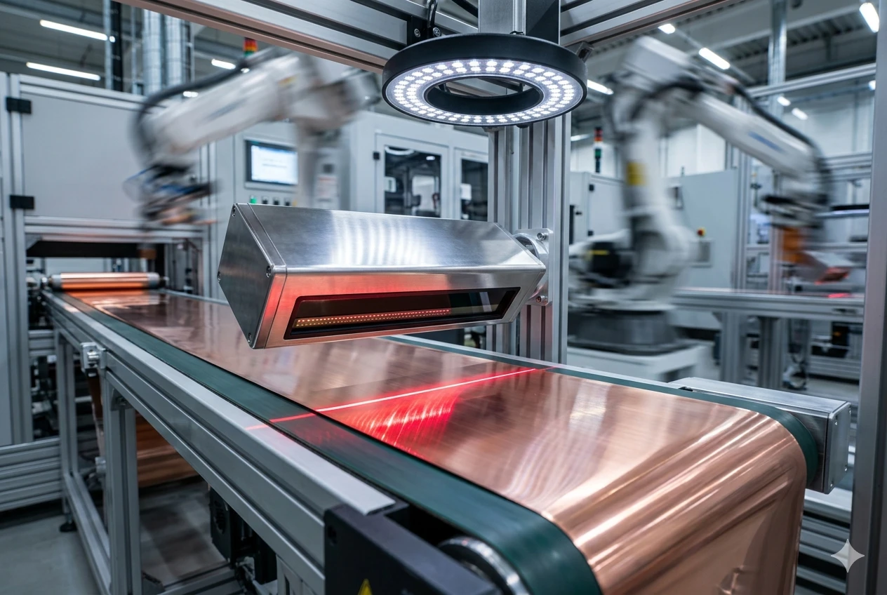
Let’s just skip the marketing fluff and get straight to the lab bench. If you are a data center hardware engineer right now, you are probably exhausted. You’re losing sleep over scaling AI server compute power. The GPUs from Nvidia and AMD are absolute beasts, the switch ASICs are pushing insane terabit throughputs, and suddenly, just getting the data from Rack A to Rack B is the hardest part of your entire system design.
Everyone in the industry talks about the heavy hitters—the 5nm DSPs, the new PAM4 modulation schemes, the fancy low-loss fiber cables. But honestly? A massive chunk of signal integrity nightmares comes down to the analog receiver end. Specifically, the detector. You can have the absolute cleanest, most pristine optical signal leaving the transmitter, but if your high speed Si PIN photodiode is garbage, you are gonna spend weeks fighting bit error rates (BER) that just won’t drop, no matter how hard your DSP works.
I’ve been in the lab at 3 AM swapping out components, burning my fingers on soldering irons, so I’m gonna give it to you straight. We need to talk about why the high speed Si PIN photodiode is the actual unsung gatekeeper of your AI server compute power, and why standard, cheap off-the-shelf detectors are basically useless for modern 400G, 800G, and 1.6T links.
The Dirty Secret of AI Server Compute Power and Thermal Walls
Here is a controversial opinion that usually gets me yelled at in meetings: Silicon Photonics (SiPh) is currently overhyped for short-reach intra-rack connections. Everyone wants to talk about integrated SiPh engines, but for sub-100 meter links inside an AI cluster, SiPh is expensive and relatively power-hungry compared to a simple, highly optimized 850nm VCSEL paired with a premium high speed Si PIN photodiode.
With the way AI clusters like the DGX systems are scaling, the power wall is our biggest enemy. Routing electrical signals across a PCB to the front-panel optics is eating up way too much power. We are hitting physical limits.
In these dense optical enviroments (yeah, they run hot), the distance between the optical engine and the switch ASIC is shrinking. For the short-reach, parallel optical links inside the rack, a silicon-based detector is the absolute best choice.
Why not Avalanche Photodiodes (APDs)? I see junior engineers suggest this all the time. APDs are a massive headache in high-density AI servers. They require high bias voltages (like 30V or more to get that avalanche multiplication), and they have terrible temperature stability. Good luck managing that in a 1RU switch chassis that runs hotter than a pizza oven. A top-tier high speed Si PIN photodiode runs on a low bias (usually 2V to 5V), is super stable across temperature swings, and frankly, is much easier to integrate alongside a broadband Transimpedance Amplifier (TIA).
Deep Dive: The Physics of the Intrinsic Layer
Let’s break down the physics real quick. No fancy formatted textbook equations, just the raw engineering math we use on the whiteboard. A high speed Si PIN photodiode has a wide, undoped (or very lightly doped) intrinsic (I) region sandwiched between heavily doped P-type and N-type semiconductor layers.
When a photon of the right wavelength hits this intrinsic region, it gets absorbed and generates an electron-hole pair. The reverse bias voltage you apply creates a strong electric field across the intrinsic region that sweeps these charge carriers away to the electrodes, creating your photocurrent.
There are two primary bottlenecks that limit the speed of your high speed Si PIN photodiode:
- Transit Time Limit: How fast the carriers physically cross the intrinsic region.
- RC Time Constant Limit: The electrical bandwidth choke based on the chip’s capacitance and resistance.
The transit time bandwidth (f_tr) is roughly approximated as:
f_tr = 0.44 * v_s / W
Where v_s is the saturation drift velocity of the carriers (around 10^7 cm/s for silicon) and W is the width (thickness) of the depletion/intrinsic region.
If you make the intrinsic region thinner, the electrons and holes have less distance to travel, meaning they cross faster, which gives you a higher f_tr. But here is the classic engineering trap: if you make it too thin, you lose Quantum Efficiency (QE) because photons just pass right through the silicon without being absorbed. Plus, bringing the P and N layers closer together acts like bringing the plates of a capacitor closer together. A thinner intrinsic region means higher junction capacitance (C_j), which absolutely ruins your RC bandwidth.
The RC bandwidth limit is calculated as:
f_rc = 1 / (2 * pi * R_L * C_total)
Where R_L is your load resistance (usually the 50-ohm input impedance of your TIA) and C_total is the total capacitance.
This is the exact trade-off that keeps us awake at night. You need a high speed Si PIN photodiode that balances the epi-layer thickness perfectly so it’s fast enough for 50G or 100G baud rates (PAM4) per lane, but still has enough responsivity to actually read the attenuated signal coming out of the fiber. At BeePhoton, we spend an absurd amount of time tweaking these MOCVD growth recipes. Generic foundry chips just don’t cut it when you are pushing this much AI server compute power.
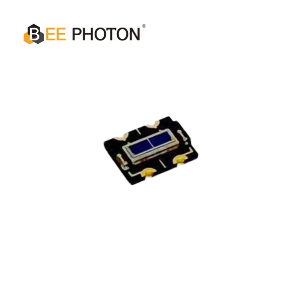
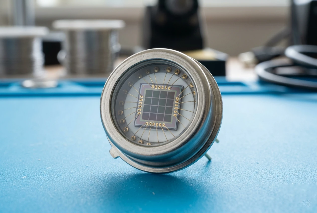
Si PIN Photodiode Array PDCA02-601
The Bee Photon PDCA Series is a precision-engineered Dual PIN Photodiode designed for high-end industrial sensing. Unlike standard single-element detectors, this silicon-based device features a segmented array structure (PD A and PD B), making it the perfect solution for differential sensing and background suppression optical switches. With a wide spectral response from 350nm to 1060nm, it ensures versatile performance across visible and near-infrared wavelengths.
Specs Hardware Engineers Actually Care About
When you are staring at a datasheet for a high speed Si PIN photodiode, you need to be skeptical. A lot of vendors quote “typical” specs under ideal lab conditions (25C, perfectly matched RF probes) that you will definetly never see in a fully populated AI server rack.
Here is what you actually need to scrutinize if you want your AI server compute power to scale without bottlenecking at the ROSA (Receiver Optical Sub-Assembly):
| Parameter | The “Legacy Telecom” Spec | The “800G AI Server” Spec | Why It Dictates System Performance |
|---|---|---|---|
| Capacitance (C_j) | 0.15 pF | < 0.05 pF | High capacitance acts as a low-pass filter, killing high frequencies. A low-capacitance high speed Si PIN photodiode is strictly mandatory to keep PAM4 eye diagrams open. |
| Dark Current (I_d) | 1 nA @ 25C | < 0.1 nA @ 25C | Dark current adds directly to your system noise floor. In hot AI racks, this spikes exponentially. You need a virtually zero baseline. |
| Responsivity (R) | 0.4 A/W | > 0.55 A/W @ 850nm | Formula: R = (η * e) / (h * v). Higher responsivity means your TIA requires less gain, lowering overall thermal noise in the receiver. |
| Bandwidth (f_3dB) | 15 GHz | > 28 GHz | For 50Gbaud PAM4, your Nyquist frequency is 25 GHz. The high speed Si PIN photodiode must comfortably pass this without severe roll-off. |
The TIA Pairing Disaster: The Wirebond Trap
A high speed Si PIN photodiode doesn’t do anything on its own. It sits right next to a TIA. I’ve seen incredibly smart hardware teams buy a top-tier high speed Si PIN photodiode and then totally ruin it by wirebonding it to a TIA with a massive, looping gold wire. This introduces parasitic inductance that completely destroys the high-frequency bandwidth.
The total input capacitance the TIA actually “sees” is:
C_total = C_pd + C_pad + C_parasitic
Where C_pd is the core junction capacitance of the high speed Si PIN photodiode, C_pad is the bond pad capacitance, and C_parasitic is the stray capacitance from the mounting epoxy and wirebonds.
But it’s not just capacitance; it’s the wirebond inductance (L_wire). If your wirebond introduces even 0.5 nH of inductance, at 25 GHz, the impedance of that tiny wire is:
Z = 2 * pi * f * L_wire = 2 * 3.14 * 25e9 * 0.5e-9 = ~78 ohms.
That 78 ohms sits right between your detector and your TIA, causing massive impedance mismatch and signal reflections. Your S21 insertion loss curve will look like a roller coaster.
If you use a bare die high speed Si PIN photodiode (which is non-negotiable for AI links), you need to minimize the wirebond length to extreme limits. Flip-chip mounting is the actual future here. By bumping the high speed Si PIN photodiode directly onto the TIA or the CPO substrate, you eliminate the wirebond inductance entirely. If you are designing next-gen hardware to maximize AI server compute power, flip-chip compatible detectors are gonna save your product line.
Real-World Case Study: Fixing a 400G SR8 Link
I won’t name the tier-1 cloud provider to protect the innocent, but they were trying to qualify a new batch of 400G SR8 transceivers for their massive new GPU training clusters. They decided to save a few pennies and used a generic high speed Si PIN photodiode from a legacy telecom supplier.
They kept failing the IEEE 802.3bs spec for Receiver Sensitivity (OMA). When we hooked up their modules to our Keysight DCA, the PAM4 eyes were completely smashed shut at the receiver DSP. Just a wall of noise.
The hardware team panicked. First they blamed the TIA. They swapped it out for a more expensive one. Same problem. They blamed the fiber. Swapped it. Same problem. They even blamed the VCSEL driver on the Tx side.
Eventually, we got them to send us the raw ROSA modules. We decapped them under the microscope and looked at the assembly. The generic high speed Si PIN photodiode they were using had an active area that was slightly too large—about 70 microns. The vendor did this to make active fiber alignment easier on the manufacturing floor, allowing them to use cheaper assembly machines. But that large active area pushed the junction capacitance up to 0.12 pF.
At 25G baud (which is 50Gbps PAM4), that 0.12 pF combined with the TIA input impedance created a brutal low-pass filter that rolled off the signal way too early. The high-frequency transition components of the PAM4 signal were literally being shaved off.
We had them desolder the ROSA and swap their detectors with a BeePhoton high speed Si PIN photodiode engineered specifically for low capacitance. We gave them our 34-micron active area bare die, which tests out at a gorgeous 0.035 pF.
The results were immediate. The RC time constant dropped off a cliff. The bandwidth opened up past 28 GHz. The TIA could actually see the high-frequency transitions, and the DSP easily equalized the remaining channel loss. Their pre-FEC BER dropped from a failing 1E-3 down to a rock-solid 1E-7.
This is why I constantly tell people you can’t just treat the high speed Si PIN photodiode as a generic jellybean component. It dictates the boundaries of your signal integrity.

Si PIN Photodiode with low dark current (350-1060nm) PDCT34-101
Discover exceptional performance with our high linearity Si PIN photodiode, designed for X-RAY and laser detection. This photodiode combines low dark current and high stability in a robust TO package. Rely on our Si PIN photodiode for critical detection tasks.
Thermal Mayhem: Dark Current in Dense AI Racks
Let’s talk about the physical enviroment. An AI server is a brutally hostile place for delicate optical components. You’ve got eight 700W GPUs sitting right next to a 51.2T switch chip. The ambient temperature inside that metal chassis is insane.
As a hardware engineer, you know the rule of thumb: dark current in a semiconductor roughly doubles every 10 degrees Celsius. If your high speed Si PIN photodiode starts with a dark current of 1 nA at 25C, by the time it hits 85C or even 105C inside the transceiver module housing, that dark current might easily push past 64 nA.
Why is that a system-killer? Shot noise.
The shot noise current formula is:
I_noise = sqrt(2 * q * (I_photo + I_dark) * B)
(Where q is the electron charge constant and B is your receiver bandwidth).
When I_dark shoots up because the rack is cooking, your noise floor rises with it. In PAM4 signaling, you have four distinct voltage levels instead of two (like in old NRZ). The vertical distance (the “eye height”) between these levels is only one-third of what it used to be. You have almost zero margin for noise. If the thermal environment of your AI server compute power pushes the dark current too high, the shot noise blurs the voltage levels, and your eye diagram collapses into garbage.
You need a high speed Si PIN photodiode with extremely low surface leakage currents. A lot of this comes down to the passivation layer on the chip. If the foundry cuts corners on the dielectric passivation step, surface leakage will completely dominate the dark current at high temperatures. We’ve spent years analyzing and refining the exact passivation recipes on our high speed Si PIN photodiode wafers just to ensure they stay dead quiet, even when the transceiver module is running at a blistering 85C case temperature.
Packaging Reality: TO-Can vs. Bare Die
If you are building low-speed 1G or 10G equipment for legacy telecom networks, sure, buy a high speed Si PIN photodiode mounted in a standard TO-46 metal can. It’s cheap, it’s robust, and you can drop it on the floor without breaking it.
But for scaling AI optical links? TO-cans are practically dead to us.
The long metal lead pins on a TO-can introduce way too much parasitic inductance. We’re talking several nanohenries, which, as I showed in the math earlier, is catastrophic at 25 GHz and above. To get the raw speed required for next-gen AI server compute power, you must use a bare die high speed Si PIN photodiode.
Handling and integrating bare die requires serious manufacturing precision. You need automated wirebonding equipment that can place ultra-short, highly repeatable wedge bonds. Or, you migrate to flip-chip bonding.
When you procure a high speed Si PIN photodiode from BeePhoton, we don’t just throw them in a bag. We supply them on UV-release tape and reel, or in specialized vacuum gel packs specifically designed for high-speed automated pick-and-place bare die bonders. We know exactly how data center hardware engineers and their contract manufacturers (CMs) need to handle these delicate components on the factory floor to maintain high yield.
Reliability: The Unseen Tax on Your AI Cluster
You know what’s worse than a part failing during qualification in your lab? A part failing in the field after you’ve deployed 10,000 AI servers in a remote data center.
Optical receivers degrade over time. It’s a sad fact of physics. A poorly manufactured high speed Si PIN photodiode might suffer from ionic drift in the passivation layer when subjected to High Temperature Reverse Bias (HTRB) conditions. Over a few thousand hours of continuous operation, the dark current slowly creeps up. At first, the DSP’s error correction (FEC) masks the issue. But eventually, the noise floor gets too high, the FEC gets overwhelmed, and the link starts dropping packets.
In an AI training cluster operating as a single massive computer, one dropped link can cause the entire distributed training job to stall, costing tens of thousands of dollars in wasted GPU compute time per hour. The long-term reliability of your high speed Si PIN photodiode directly dictates the financial ROI of your AI server compute power.
We run brutal Telcordia GR-468 qualification tests on every single batch. Damp heat (85C / 85% RH), severe thermal shock cycling, accelerated aging. If a high speed Si PIN photodiode wafer shows even a hint of dark current drift after 2000 hours of stress testing, we scrap the entire wafer. Period. You shouldn’t accept anything less rigorous from your component supplier. Infant mortality in your ROSA is unacceptable at this scale.
The DSP Interplay: Saving Megawatts of Power
So, your high speed Si PIN photodiode catches the 850nm light, converts it to current, hands it to the TIA to become voltage, and then what? It hits the DSP (Digital Signal Processor).
Back in the old 10G NRZ days, you could get away with simple analog CDRs (Clock and Data Recovery circuits). Now, with 50G and 100G PAM4 lanes, heavy digital DSPs are mandatory just to clean up the dispersed signal. They use complex equalization algorithms—FFE (Feed-Forward Equalization) and heavily tapped DFE (Decision Feedback Equalization).
But DSPs are massive power hogs. They generate tons of heat and consume precious watts. The cleaner the analog signal coming out of your high speed Si PIN photodiode and TIA combo, the less tap equalization the DSP has to mathematically perform. If you use a premium, ultra-high-bandwidth high speed Si PIN photodiode, you can actually configure your DSP firmware to run with fewer active taps.
Fewer taps = less switching activity in the silicon = less power consumed.
In a massive hyperscale data center, saving just 0.5 to 1 watt per optical transceiver link translates to literally megawatts of power saved across the entire facility. That is critical power that can be redirected back to the GPUs to increase your raw AI server compute power. It’s all fundamentally connected. Your choice of a microscopic high speed Si PIN photodiode ripples all the way up to the facility’s master power envelope.
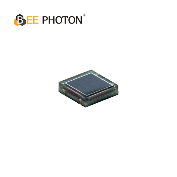
Si PIN Photodiode with NIR sensitivity enchanced (350-1100nm) PDCC34-501
Bee Photon offers a High Stability PIN Photodiode for precise industrial sensing. This NIR enhanced photodiode ensures reliable measurements from 350-1100nm. A top choice for a high stability photodiode.
Stop Guessing with Your Signal Integrity
Look, the supply chain is flooded with cheap optics right now. It’s incredibly tempting for procurement teams to try and cut costs on the analog receiver side. Don’t let them do it to your design.
When you are speccing out the BOM for your next 400G, 800G, or 1.6T module, you need to partner with a detector company that actually understands high-frequency RF microwave design and hardcore semiconductor physics, not just a catalog distributor.
You need a high speed Si PIN photodiode that:
- Defends your bandwidth with a junction capacitance firmly under 0.05 pF.
- Uses top-tier proprietary passivation for ultra-low dark current even at 85C+.
- Is easily available in bare die formats to accomodate short-wirebond or modern flip-chip packaging.
- Can handle the massive optical overload from short-reach VCSEL arrays without collapsing into saturation.
If you are a hardware engineer tasked with pushing the absolute boundaries of AI server compute power, you need analog components that won’t let your DSP down. Check out our full lineup of high speed Si PIN photodiodes to see exactly what I’m talking about. We engineered these chips specifically to solve the exact headaches I’ve just ranted about.
Frequently Asked Questions (FAQ)
Why is a high speed Si PIN photodiode preferred over InGaAs for AI server links?
Most intra-rack AI server links use Multimode Fiber (MMF) paired with 850nm VCSELs because it is vastly cheaper and uses significantly less power for short distances (typically under 50 to 100 meters). Silicon (Si) has near-perfect absorption characteristics at the 850nm wavelength. InGaAs detectors are optimized for 1310nm or 1550nm wavelengths over Single Mode Fiber (SMF) for long-haul distances. So for the dense mesh of connections inside the AI rack, a silicon-based high speed Si PIN photodiode is by far the most efficient, cost-effective, and performant choice.
How does active area size affect the high speed Si PIN photodiode performance?
It is a direct, brutal trade-off. A larger active area (e.g., 70um) makes it way easier to mechanically align the optical fiber to the high speed Si PIN photodiode, which lowers your manufacturing and assembly costs. However, a larger area directly increases the junction capacitance, which tanks your high-frequency bandwidth. For 50G/100G lanes, you generally have to shrink the active area down to around 30um-40um to keep the capacitance low enough. This means your contract manufacturer needs much better active alignment tolerances.
Can I test a bare die high speed Si PIN photodiode before wirebonding it?
Yes, but it requires specialized RF probe stations. You can use high-frequency coplanar RF probes (like GSG probes) to measure the S-parameters (specifically S11 return loss and S21 bandwidth) of the bare die high speed Si PIN photodiode right on the wafer or while it’s sitting in a gel pack. This allows hardware engineers to verify the bandwidth and parasitic capacitance before committing the chip to an expensive TIA substrate. We do this exact probing routinely at BeePhoton before shipping.
What is the maximum optical input power a high speed Si PIN photodiode can handle?
This is known as the saturation limit. If you blast a high speed Si PIN photodiode with too much optical power (which can happen on very short 2-meter links), the internal electric field physically collapses because of the sheer volume of generated carriers (known as the space charge effect). When this happens, the speed drops off a cliff, and the signal heavily distorts. Most premium high speed Si PIN photodiodes can handle up to +3 dBm or +5 dBm of average optical power, but you need to check the peak optical power of your specific PAM4 signal to ensure it doesn’t cause transient saturation.
Ready to Fix Your BER Issues?
Are you tired of chasing ghost BER issues in your optical receivers? If your current detectors are holding back your AI server compute power and driving your DSPs to the breaking point, it’s time to upgrade your BOM.
We don’t just sell generic chips; we engineer custom silicon solutions for data center hardware engineers who need things to work flawlessly the first time. We can fully customize the active area, the RF pad layout, and the epilayer thickness of your high speed Si PIN photodiode to perfectly match your specific TIA impedance and packaging constraints.
Don’t let a poorly spec’d detector ruin your 800G rollout.
Shoot us an email with your TIA input specs and your target baud rate. Let’s get your links running flawlessly.
Email me and the core engineering team directly at info@photo-detector.com or visit our Contact Us page to request bare die samples and full S-parameter test data.
BeePhoton – Engineered for the Speed of AI. (Check out our main site at https://photo-detector.com/)