If you’ve ever messed around with phototransistors in a project, you know they can stop working outta nowhere. Turns out, a lot of times its just static electricity zapping them when you least expect it. Those little sparks you dont even feel can fry the sensitive parts inside. Ive seen it happen plenty – one minute everythings fine, next minute the sensor’s acting weird or dead completely.
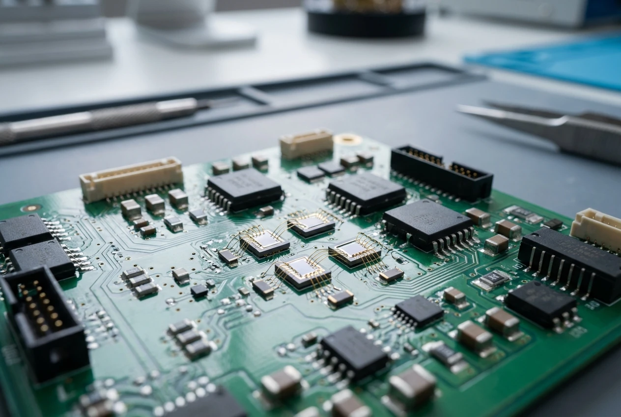
Phototransistors are super useful for detecting light in all kinds of stuff, like remote controls, proximity sensors, or even industrial automation setups. But theyre kinda fragile when it comes to electrostatic discharge, or ESD for short. Thats why getting phototransistor ESD protection right matters a ton if you want reliable performance over time.
In this guide, we’ll walk through what ESD really does to these devices, how to spot static damage early, and practical ways to keep them safe. I’ll share some tips we’ve picked up over years at Bee Photon working with optical components. By the end, youll have solid steps to follow so your phototransistors last longer and perform better.
What ESD Is and Why Phototransistors Hate It
ESD happens when static charge builds up and then jumps suddenly – like when you shuffle across carpet and touch a doorknob. Your body can carry thousands of volts without you noticing, but for tiny semiconductor devices like phototransistors, even a few hundred volts is enough to cause trouble.
According to the ESD Association, many electronic components get damaged by discharges below 100 volts. Optical sensors, including phototransistors, often fall into Class 1 sensitivity under the Human Body Model (HBM) testing in JEDEC standards like JS-001 – meaning they can fail at voltages as low as 250-500 volts in real-world handling.
The problem comes from the thin junctions inside the transistor that convert light to current. A quick zap melts or weakens those layers, leading to permanent issues. Weve tested batches here and found untreated devices failing way more often in dry environments where static builds easier.
Humidity plays a big role too – below 30% relative humidity, static charges stick around longer and discharge harder. Thats why labs and factories keep humidity higher when handling optical components.
Spotting Signs of Static Damage in Phototransistors
Catching ESD damage early saves headaches later. Heres what to watch for:
- Reduced sensitivity → The device doesnt respond as strongly to light. You might need brighter sources to get the same output, or it drifts over time.
- Increased dark current → Leakage even with no light hitting it. Thats a classic sign of junction breakdown from static damage.
- Complete failure → No output at all, or erratic behavior like random spikes.
- Shifted characteristics → The peak wavelength response moves, or gain drops off.
In one assembly line we helped troubleshoot (keeping it anonymous), devices were failing tests at a 15% rate. Turned out workers werent grounded properly, and microscopic exams showed tiny melt spots on the dies – textbook ESD hits.
Sometimes damage is latent, meaning it works at first but fails sooner under stress. Studies on similar optical devices, like VCSELs in optics journals, show ESD weakening bonds that lead to early degradation.

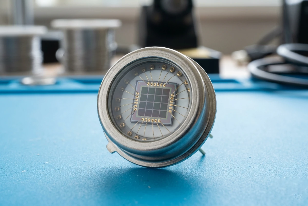
Si phototransistor PTCP Series PTCP001-102
High-sensitivity Silicon Phototransistor designed for precision detection in the 800-1100nm spectral range. This black plastic IR sensor ensures minimal noise and high reliability. Ideal for industrial applications requiring a robust silicon phototransistor with excellent response speed.
Best Practices for Handling Optical Components Safely
Handling optical components right is half the battle for good phototransistor ESD protection. Heres what actually works based on real setups:
- Always use an ESD wrist strap connected to ground. Clip it to a verified earth point, not just any metal.
- Work on an anti-static mat with a ground cord. These dissipate charges slowly instead of letting them spark.
- Wear heel straps if youre moving around a lot.
- Keep devices in conductive bags or trays when not in use. Never toss them loose on a bench.
- Avoid synthetic clothes that generate static – cotton’s better.
- Ionizers help in dry areas by neutralizing air charges.
We set up workstations like this at our facility, and failure rates dropped dramatically. Simple stuff, but consistent.
For storage and shipping, use moisture barrier bags with ESD shielding. Label them clearly so everyone knows to handle carefully.
Quick Comparison of Common ESD Protection Tools
| Tool/Method | How It Helps | Cost Level | Ease of Use | Best For |
|---|---|---|---|---|
| Wrist Strap + Mat | Direct grounding for person and surface | Low | Easy | Daily bench work |
| Ionizer | Neutralizes airborne charges | Medium | Moderate | Dry environments |
| Conductive Bags/Trays | Shields during storage/transport | Low | Very Easy | Shipping and inventory |
| Humidity Control | Reduces static buildup overall | High | Ongoing | Full production lines |
| ESD-Safe Packaging | Built-in protection for components | Medium | Easy | Supplier to customer |
This table shows theres no one-size-fits-all, but combining a couple covers most risks.
Setting Up Proper ESD Protection for Sensors
When building systems with phototransistors as sensors, think beyond just handling – protect them in the final design too.
Some modern phototransistors come with better inherent robustness, but adding external protection helps. TVS diodes or varistors across pins clamp surges.
At Bee Photon, our silicon phototransistors are designed with reliable packaging that handles typical ESD better than older types. Customers tell us they see fewer field returns after switching.
Ground your PCB properly with a solid plane, and route sensitive traces away from edges where discharges enter.
In automated assembly, use ionized air blowers over pick-and-place areas. One client in automation cut defects by 80% just adding that.
Step-by-Step Guide to Protecting Phototransistors During Work
Heres a straightforward routine we follow:
- Before starting, test your wrist strap – should read under 1 megohm to ground.
- Clear the bench of insulators like plastic cups or paper.
- Unpack devices only at the grounded station.
- Hold by the body, not leads – or use tweezers if needed.
- Insert into boards carefully, avoiding sliding across surfaces.
- After soldering, test immediately for basic function.
- Store leftovers back in shielded packaging right away.
Takes an extra minute, but prevents hours of debugging later.
Real-World Scenarios Where Good ESD Habits Made a Difference
Over the years, we’ve seen projects turn around with better practices.
One team building medical sensors kept getting inconsistent readings. Traced it to handling on non-ESD benches during prototyping. Switched to proper mats and straps, plus our silicon phototransistors, and reliability shot up – devices lasting full expected life in field trials.
Another case involved industrial light barriers failing intermittently in dry factory air. Added humidity control and ionizers around assembly, plus choosing components rated higher for ESD. No more random failures, production yields improved noticeably.
These arent rare – ESD costs the electronics industry billions yearly, per industry reports. But simple fixes work wonders.

Si phototransistor PTCP Series PTCP001-202
Enhance your switching solutions with this 800-1100nm NPN Phototransistor. Perfect for photoelectric switches, it offers high power dissipation up to 90mW. This silicon phototransistor delivers consistent performance in harsh environments from -40°C to +85°C.
Choosing Reliable Phototransistors for Tough Environments
If youre sourcing new parts, look for ones tested to higher HBM levels – at least 1kV or more.
Our lineup at Bee Photon focuses on durable silicon phototransistors that perform well even in challenging setups. Check out the details on our silicon phototransistor product page – theyre built keeping real-world handling in mind.
Pair them with good practices, and you get sensors that just work, longer.
Frequently Asked Questions About Phototransistor ESD Protection
Whats the most common way phototransistors get ESD damage?
Usually from human handling without grounding. Even touching leads after walking across a room can zap them if statics high.
Can ESD-damaged phototransistors be fixed?
Nope, damage is permanent. Best to prevent it upfront.
Do all phototransistors need the same level of protection?
Pretty much yes – most are sensitive, but some packaged versions handle more. Always treat them carefully.
How do I know if my workspace is ESD-safe?
Test with a meter for resistance to ground, and use a static field meter to check charges. Under 10^9 ohms surface resistivity is good for mats.
Are there ESD protection sensors built into some devices?
Some advanced ones have internal clamping, but for standard phototransistors, external habits are key.
If you got more questions or need help picking parts, drop us a line.
Wrapping It Up – Keep Your Phototransistors Safe
Protecting phototransistors from ESD boils down to awareness and consistent habits. Ground yourself, control the environment, handle carefully – and choose solid components.
At Bee Photon, weve helped tons of folks get better reliability with our optical detectors. If youre dealing with static issues or just want tougher sensors, reach out.
Head over to our contact page or email info@photo-detector.com for a quote or chat about your setup. Wed love to help make your project more reliable.