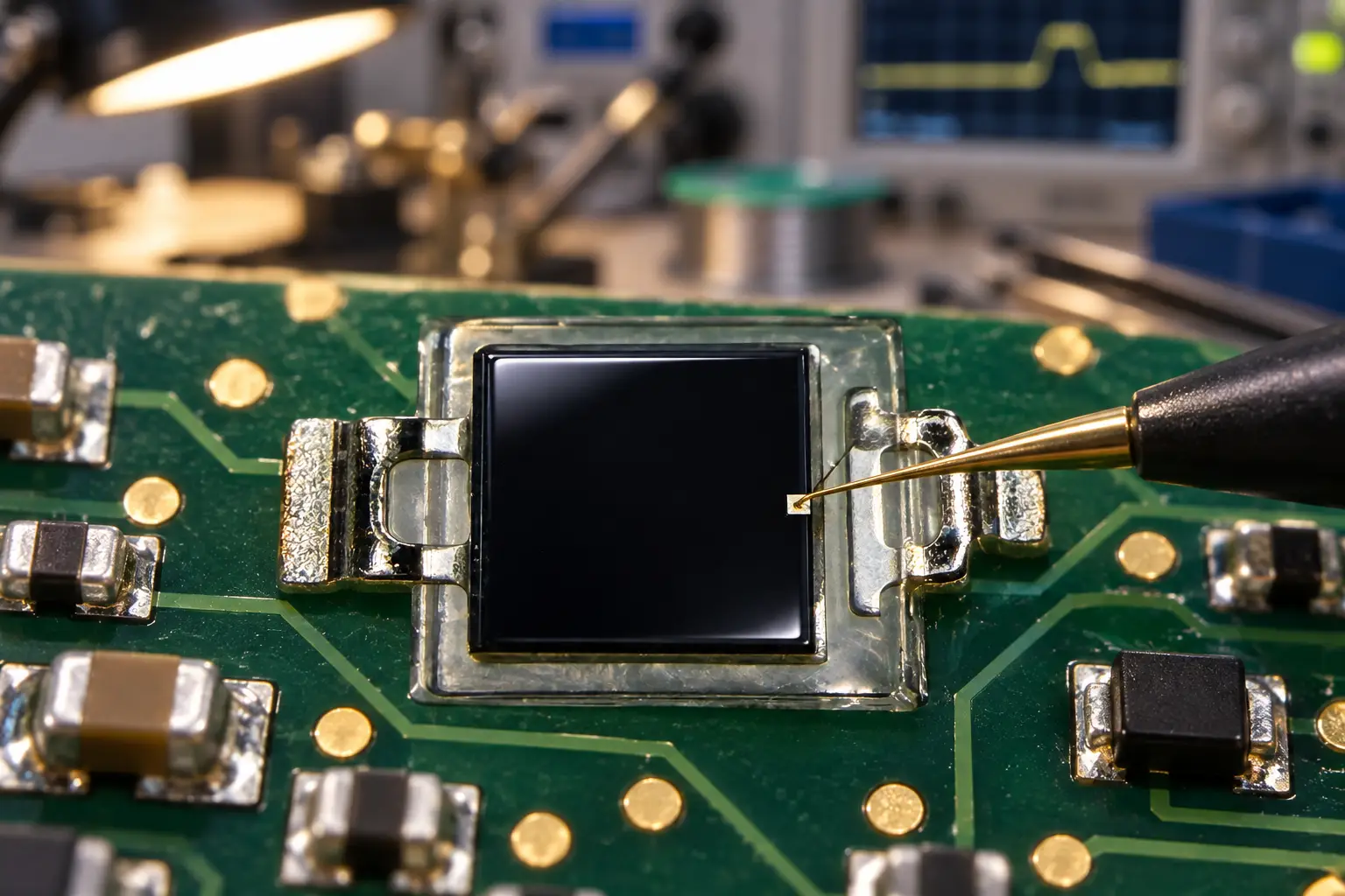
Last month a hardware engineer pinged me on LinkedIn, pulling his hair out over an automated sorting line. The setup kept dropping optical packets whenever ambient warehouse high-bays kicked on, yet on the bench, the receiver circuit worked flawlessly. After five minutes reviewing their bill of materials, the culprit stuck out immediately: they paired an 850nm-biased photodetector with an emitter rated at 940nm and tried to compensate by cranking up the transimpedance gain.
If you design industrial light curtains, optical gates, liquid-level switches, or machine safety barriers, choosing your 940nm IR receiver diode should never be treated as an afterthought. It determines your signal-to-noise ratio, optical alignment margin, and how hard your emitter has to work.
Let’s cut past generic distributor data sheets and talk about what matters when pairing a silicon detector with an active emitter in a through-beam optical system.
Quick benchmark: In dirty factory environments with dust and high ambient lux, operating at 940nm instead of 850nm cuts solar and ambient visible noise drastically because ambient sunlight drops sharply near the water absorption band around 940nm. But if your 940nm IR receiver diode lacks a matched day-light filter, you toss that physical advantage straight out the window.
Why 940nm IR Receiver Diode Choices Make or Break Through-Beam Sensing
In a classic through-beam sensor (sometimes called an opposed-mode sensor), your emitter and detector face each other directly across an air gap. The target breaks the beam. It sounds dead simple until you remember that every stray photon from overhead fluorescent bulbs, LED work lights, or sunlight bounces directly into your receiver’s aperture.
Here is the dirty reality: Silicon naturally hits its peak responsivity around 850nm to 900nm. When you push your emitter to 940nm to avoid the annoying faint red glow visible at 850nm, standard silicon drops in baseline responsivity.
If you just pick a random detector off an online catalog without looking at spectral alignment, you end up needing massive op-amp gains. And huge gain introduces phase shift, thermal drift, and picking up RF garbage from nearby brushless motors. You want the highest possible optical efficiency right at the die and packaging level before your signal touches an amplifier.
1. Peak Spectral Matching: Stop Burning Gain on Mismatched Curves
The biggest headache in photodiode circuits is spectral mismatch. Every LED emitter pumps out light across a Gaussian spectral envelope with a full-width at half-maximum (FWHM) typically between 30nm and 50nm.
A good 940nm IR receiver diode must match that bell curve. Take a look at standard silicon PIN photodiodes; bare silicon responds from roughly 400nm all the way to 1100nm. If you drop clear epoxy packaging into an industrial floor, ambient room light swarms the junction. Your detector saturates into DC clipping, or your dynamic range shrinks to nothing.
Daylight Blocking Filters: Black Epoxy vs. Clear Epoxy
For practical optical gates, you almost always want black cast epoxy. Black epoxy acts as a built-in optical high-pass or bandpass filter, blocking visible light below 750nm or 800nm while letting 940nm slide through with minimal attenuation.
- Bare / Clear Plastic: Wide response (400nm–1100nm). Fantastic for medical pulse-ox where you want multiple wavelengths, terrible for through-beam machine sensors.
- Black Epoxy / Visible Blocking: Filters out visible noise. When paired with a black epoxy PIN photodiode, the noise floor drops instantly, letting you run a lean, high-speed amplifier circuit without random false triggers from overhead shop lights.
If you don’t use daylight filtering on the component level, you will end up adding expensive external optical bandpass windows to your sensor housing, raising unit BOM costs unnecessarily.

Si PIN photodiode PDCP08 Series PDCP08-511
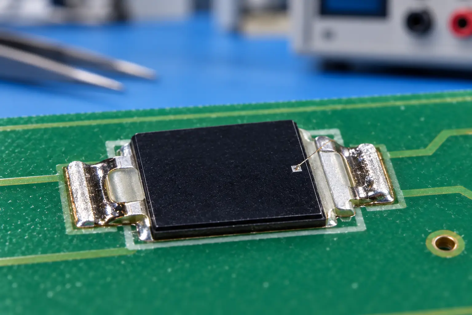
The PDCP08-511 is a high-performance Black Epoxy PIN Photodiode designed for precision infrared applications. Encased in a special black epoxy resin, this sensor effectively acts as a daylight filter, blocking visible light interference while maximizing sensitivity at 940nm. With a large 2.9×2.9mm active area and low dark current, it ensures reliable signal detection for optical switches and remote control systems, even in noisy ambient light environments.
2. Responsivity (A/W): The Real Math Behind Signal Strength
Data sheets love boasting about open-circuit voltage or short-circuit current under arbitrary light conditions (like standard Illuminant A at 2856K). Ignore those tungsten lamp ratings. They mean practically nothing when driving the part with an LED emitter.
What you need to check is Spectral Responsivity, labeled as R_lambda, measured in Amperes per Watt (A/W).
Responsivity Formula and Quantum Efficiency
Responsivity connects directly to Quantum Efficiency (QE):
Responsivity (R_lambda) = (q * lambda * QE) / (h * c)
Where:
- q = electron charge (1.602 x 10^-19 Coulombs)
- h = Planck’s constant (6.626 x 10^-34 J*s)
- c = speed of light (3.0 x 10^8 m/s)
- lambda = wavelength in meters (940 x 10^-9 m)
- QE = Quantum Efficiency (percentage of photons that create electron-hole pairs)
Plugging those physical constants in gives you the practical shortcut formula:
R_lambda = (lambda in micrometers / 1.24) * QE
At 940nm (0.94 um), if your detector has a theoretical 100% quantum efficiency, maximum responsivity would hit about 0.758 A/W. In the real world, Fresnel reflections at the silicon boundary, junction depth, and epoxy absorption pull this down.
A high-grade 940nm IR receiver diode typically achieves between 0.55 A/W and 0.65 A/W at 940nm. If you look at a part whose peak sits at 850nm (where it scores 0.62 A/W) and you check its curve down at 940nm, it might plummet to 0.35 A/W.
That 40% loss forces you to either pump more current through your emitter LED (killing its lifespan and battery budgets) or double the value of your feedback resistor in the transimpedance amplifier (TIA), which cuts your bandwidth and jacks up thermal Johnson noise.
Optical Signal Chain: Incoming Photons (P_opt at 940nm) -> Optical Filter Epoxy (blocks visible noise below 750nm) -> Silicon PIN Junction (QE around 75% to 85%) -> Generated Photocurrent: I_ph = P_opt * R_lambda
If you need a reliable compact detector with tight responsivity tolerances across production batches, the 2.9×2.8mm silicon PIN photodiode is a workhorse candidate for compact edge-detection gates.
3. Directivity and Viewing Angle: Mechanical Tolerance vs. Crosstalk
Here is an area where mechanical teams and electrical teams routinely get into fights: the half-angle (theta 1/2) or viewing angle of the 940nm IR receiver diode.
A through-beam sensor can be configured with two optical philosophies:
- Narrow Beam / Focused Lens (+/- 15 to 20 degrees): Great for long sensing distances (over 5 meters). Gives a strong signal because light is concentrated onto the active silicon area. But if the mounting bracket vibrates or gets nudged by an operator, you lose beam alignment completely.
- Wide Beam / Flat Lens (+/- 55 to 65 degrees): Highly forgiving during mechanical installation. Ideal for short gaps (10mm to 500mm), such as paper detection in printers or slot sensors. The penalty? It sees more optical bounce off surrounding machinery and can be blinded by adjacent sensor channels.
Acceptance Angle Comparison
| Package Style | Typical Half Angle (theta 1/2) | Best Sensing Range | Mechanical Alignment Difficulty | Risk of Optical Crosstalk |
|---|---|---|---|---|
| Dome Lens (T-1 3/4 5mm through-hole) | +/- 15 deg to +/- 25 deg | 2m to 15m | High (requires precision mounts) | Low |
| Side-Looker Molded Package | +/- 30 deg to +/- 45 deg | 0.5m to 3m | Moderate | Medium |
| Flat SMT Top-View (e.g., 1206 or mini-leadless) | +/- 60 deg to +/- 75 deg | 5mm to 1m | Very Low (easy drop-in) | High (requires baffling) |
When you lay out multi-channel through-beam barriers (like an array of optical inputs checking the height of boxes on a conveyor), wide-angle diodes will catch stray pulses from their neighboring emitters. You either have to install physical honeycomb baffles or multiplex the emitters in firmware so only one channel fires at any single microsecond.
For dense arrays, choosing a narrow profile like the silicon PIN photodiode helps prevent optical bleed without overcomplicating the mechanical enclosure.
4. Reverse Bias, Junction Capacitance, and Response Time
A common rookie mistake: treating a photodiode like a passive photoresistor (LDR). Photodiodes in through-beam systems are usually wired in either photovoltaic mode (zero bias) or photoconductive mode (reverse bias).
For precision and zero dark current drift, zero bias sounds great on paper. But for high-speed beam breaking—say, calculating the RPM of a turbine or spotting tiny drops in high-speed dispensing—zero bias will kill your edge speed due to high junction capacitance (C_j).
Junction capacitance acts as a low-pass filter with your transimpedance feedback network:
Cutoff Frequency (f_3dB) = 1 / (2 * pi * R_f * C_total)
Where:
- R_f = Feedback resistor of the TIA
- C_total = C_junction + C_amplifier_input + C_stray_pcb
When you apply a reverse bias (e.g., V_R = 5V or 12V), you widen the depletion layer inside the PIN structure (the intrinsic “I” layer). That drastically shrinks C_j, dropping rise time from microseconds down to single-digit nanoseconds.
Dark Current Trade-Off
Nothing comes for free in analog hardware. When you increase reverse bias on your 940nm IR receiver diode, you increase reverse dark current (I_D):
- Increasing Reverse Bias (V_R): Junction Capacitance (C_j) decreases, enabling faster rise/fall times.
- The Downside: Dark Current (I_D) increases, raising the DC offset voltage and shot noise floor.
According to fundamental solid-state physics outlined in technical publications by the National Institute of Standards and Technology (NIST), dark current doubles approximately every 8 to 10 degrees Celsius rise in temperature. If your through-beam optical system lives inside a hot manufacturing enclosure reaching 60 deg C, an aggressive reverse bias can create a substantial DC drift.
Make sure your downstream transimpedance stage uses AC-coupling if you are pulsing your emitter, or implement active baseline cancellation in software.
5. Circuit Architectures: TIA Design for Noisy Environments
Too many sensor designs fail simply because the transimpedance amplifier wasn’t stabilized. When a photodiode’s junction capacitance hangs off the inverting input of an operational amplifier, it adds a pole to the loop-gain curve, creating a phase lag that often results in ringing or outright parasitic oscillation.
Feedback Network Overview: The photodiode connects to the inverting op-amp terminal, where a feedback resistor (R_f) converts photocurrent to output voltage. To prevent instability, a parallel feedback capacitor (C_f) cancels phase lag caused by the photodiode junction capacitance, while the non-inverting terminal stays tied to ground or a quiet reference voltage.
To stabilize your 940nm IR receiver diode circuit, always place a small feedback capacitor (C_f) in parallel with R_f. You can estimate the minimum value needed to prevent instability with this standard relationship:
C_f = sqrt( C_in / (2 * pi * R_f * GBW) )
Where:
- C_in = Total input capacitance (Photodiode C_j + Op-Amp common-mode & differential capacitance + layout parasitics)
- GBW = Gain Bandwidth Product of your operational amplifier
If you skip C_f, your through-beam sensor might operate fine on your test bench at room temperature, but it will chatter or oscillate when ambient temperature shifts the photodiode parameters.
For engineers looking for deeper mathematical rigor on amplifier noise optimization, Texas Instruments application note on TIA stability remains an essential piece of technical reading.

Si PIN photodiode PDCP08 Series PDCP08-502
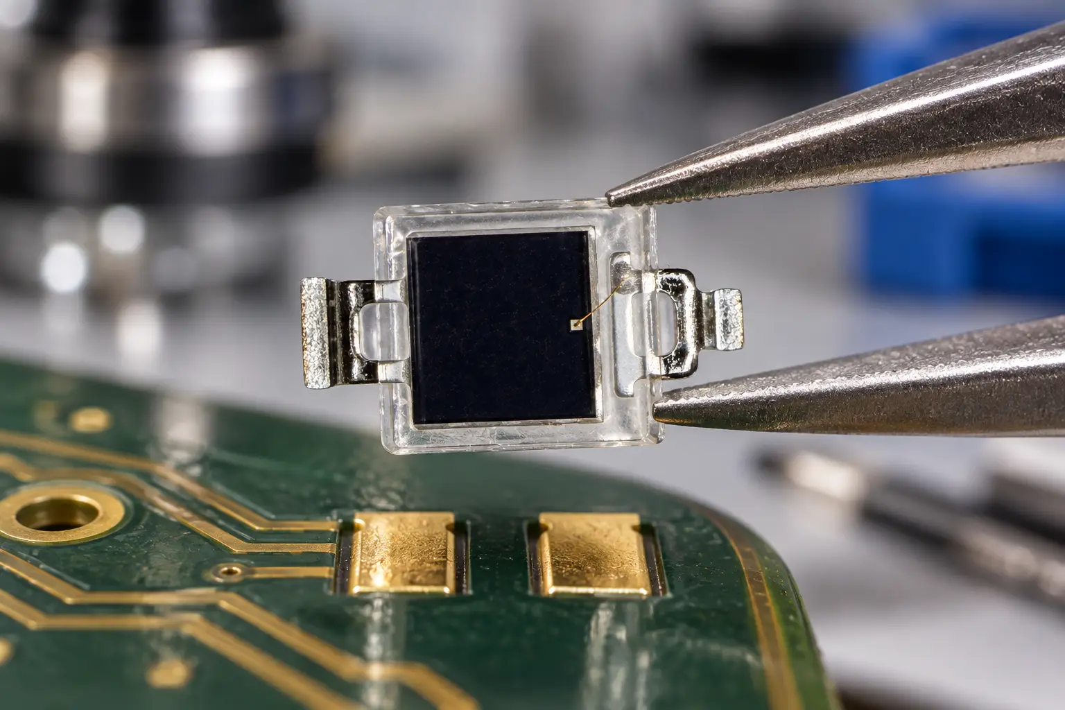
The PDCP08-502 is a high-response 2.9×2.8mm Silicon PIN Photodiode designed for precision photoelectric applications. Featuring low junction capacitance, low dark current, and a wide spectral range (340-1100nm), it is the ideal component for optical switches and compact sensing modules requiring stable and fast signal output.
Real-World Case Study: Fixing Ghost Triggers in a Packaging Sorter
A factory automation builder in Michigan was building a dual-lane carton sorting gate. They used through-beam optical arrays spaced 40mm apart to measure the silhouette of passing packages.
The Symptom
Every time two reflective white cartons passed adjacent channels simultaneously, Channel 2 would throw a false “beam broken” signal even when no carton was in its path.
The Diagnostic
The engineering team assumed their firmware pulse-detection code had a timing bug. But an oscilloscope hooked to the photodiode cathode showed an unwanted pulse train synchronized with the Channel 1 LED emitter.
The original design used wide-angle flat SMT photodiodes (+/- 65 deg) with clear packaging. Light from Channel 1’s emitter was bouncing off the glossy carton exterior into Channel 2’s wide receiver. Furthermore, the clear epoxy was picking up harmonics from overhead high-pressure sodium fixtures.
The Fix
We reworked the front end:
- Swapped the generic detector for a dedicated 940nm IR receiver diode with an integrated black daylight filter.
- Selected a tighter viewing angle package (+/- 25 deg) using BeePhoton photodiode components to mechanically reject wide-angle bounce.
- Shifted the transimpedance amplifier from DC-coupled raw thresholding to an AC-coupled bandpass topology tuned to the emitter’s 10kHz burst frequency.
Result: Crosstalk dropped below the sensor’s noise floor, false trips disappeared entirely, and the sorting line ran clean at 120 units per minute.
Key Mistakes to Avoid When Specifying Your 940nm Photodetector
- Trusting “Peak 940nm” marketing claims blindly: Always inspect the spectral curve in the datasheet. Some vendors rebrand general silicon photodiodes (peak ~880nm) as “940nm detectors” simply because they have roughly 70% responsivity left at 940nm. True 940nm-optimized silicon tweaks the doping and anti-reflective coating to maximize responsivity specifically at that wavelength.
- Ignoring Active Area Trade-offs: A large active area (e.g., 5mm x 5mm) collects tons of photons, making optical alignment forgiving. However, capacitance scales directly with surface area. A giant die will kill your response time. If you need switching speeds faster than 1MHz, pick an active area under 1mm^2 and use proper mechanical lenses.
- Forgetting Solder Profile Sensitivity: Miniature optical packages with dyed epoxy are sensitive to thermal profiles. Exceeding reflow temperature limits per IPC/JEDEC J-STD-020 standards can cause micro-cracks in the filter resin, introducing moisture, degrading responsivity, or shifting the optical acceptance angle.
- Confusing Phototransistors with Photodiodes: If your through-beam gate needs microsecond response times, do not use a phototransistor. Phototransistors give you internal current gain, yes, but their Miller capacitance will drag your switching frequencies down into the low tens of kilohertz. Stick with a quality 940nm IR receiver diode and an external op-amp.
Testing Your 940nm Through-Beam Sensor Under Real Conditions
Bench tests inside an R&D lab with comfortable fluorescent lighting never tell the whole story. Before releasing your PCB to production, test your 940nm IR receiver diode against these real-world stressors:
- Direct Strobe Interference: Fire a modern high-intensity LED flashlight directly into the aperture while transmitting pulses. Your circuit should reject the DC or 120Hz ripple without railing the amplifier.
- Thermal Drift in Dark Current: Place the detector in a thermal chamber at 70 deg C (or your product’s maximum operating rating). Verify that the dark current doesn’t shift the baseline past your comparator’s switching threshold.
- Dust and Attenuation Margin: Drop an optical neutral-density filter (or a semi-translucent plastic sheet) between emitter and receiver to simulate years of industrial dust accumulation. A robust through-beam design should have at least a 10x (10dB) optical excess gain margin.
Refer to the testing guidelines by the International Electrotechnical Commission (IEC 60947-5-2) for industrial proximity switches and optical sensors to ensure your functional tests match regulatory standards.
Summary Checklist for Hardware Engineers
When you finalize your component selection, run down this quick checklist:
- Does the receiver have an integrated daylight-blocking filter for 940nm?
- Is the spectral responsivity at least 0.55 A/W at 940nm?
- Is the half-angle matched to your mechanical vibration tolerance without causing crosstalk?
- Is the junction capacitance low enough to hit your required cutoff frequency with chosen feedback values?
- Have you accounted for dark current rise over your full operating temperature range?
Getting your 940nm IR receiver diode selection right on day one saves countless redesign cycles, field recalls, and awkward discussions with manufacturing plant managers.
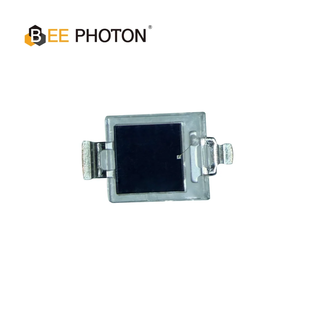
Si PIN photodiode PDCP08 Series PDCP08-501
High-Performance Detection: The PDCP08-501 is a high-speed Silicon PIN Photodiode with a transparent window.
Key Specs: Featuring a 2.9×2.9mm active area, this PIN photodiode offers low dark current and high responsivity, making it an ideal sensor for general optical switches and light detection systems.
Frequently Asked Questions (FAQ)
Can I use an 850nm LED emitter with a 940nm IR receiver diode?
Technically, yes, but it is deeply inefficient. If your receiver diode uses black epoxy optimized for 940nm, it might block or significantly attenuate 850nm light depending on the cut-on wavelength of the daylight filter. Even with clear packaging, mismatching the peak emitter wavelength will reduce your link margin by 30% to 50%, forcing you to boost power consumption elsewhere.
Why is 940nm preferred over 850nm in human-adjacent safety through-beam gates?
Two main reasons: visual stealth and sunlight rejection. 850nm emitters exhibit a visible, dull red glow that can distract operators or look unappealing in consumer applications. 940nm is completely invisible to the naked human eye. Additionally, solar irradiance hitting the earth’s surface has a natural atmospheric absorption dip near 940nm, meaning less solar background noise outdoors or near windows.
How does reverse bias voltage affect the durability of a 940nm IR receiver diode?
As long as you stay well within the absolute maximum ratings specified on the manufacturer datasheet (typically 20V to 30V for PIN photodiodes), reverse biasing does not degrade silicon life. However, excessive bias increases continuous dark current and localized power dissipation inside the die. If operated near maximum thermal limits, that extra heat can accelerate long-term packaging degradation.
Build Your Next Optical Sensor With BeePhoton
Are you designing a custom through-beam optical gate, liquid level monitor, or industrial light curtain? Getting the optical pairing right between your emitter and your 940nm IR receiver diode requires practical experience with real silicon behaviors, active die areas, and custom optical packaging.
At BeePhoton, we engineer and manufacture high-performance silicon PIN photodiodes, phototransistors, and custom optical sensors tailored to tough industrial environments. Whether you need daylight-filtered black epoxy packages, custom die shapes for narrow arrays, or drop-in alternatives to cut BOM costs:
- Explore our full product lineup at BeePhoton Official Website.
- Need advice on matching responsivity and viewing angles for your circuit? Contact the BeePhoton Engineering Team or send your schematics and optical gap specs directly to info@photo-detector.com. Let’s make sure your optical front-end is reliable from the first prototype run.