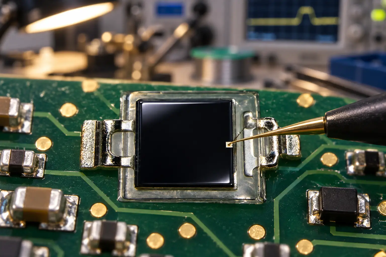
Trying to squeeze an optical sensor into a 4 mm medical probe, a sleep-tracking smart ring, or a miniature industrial slotted switch quickly turns into an exercise in frustration. Standard SMD photodiode footprints like 0805 or 1206 gobble up critical routing corridors. Worse yet, large packages introduce excessive parasitic junction capacitance, which kills amplifier bandwidth and forces ugly power compromises.
When board space disappears, opting for a miniature PIN photodiode 1.1×1.1 becomes the most viable route forward. Shrinking silicon down to a 1.1 mm by 1.1 mm footprint lets you squeeze dual-wavelength reflectance channels, micro-aperture beam-breaks, and dense detector arrays into enclosures once considered impossible.
However, cramming silicon into tiny packages brings its own challenges. You trade package bulk for tight tolerances, tricky solder fillet dynamics, and unforgiving board parasitics. Let’s look at real-world integration strategies, bench math, and layout lessons learned from deploying the miniature PIN photodiode 1.1×1.1 in compact sensing platforms.
What Makes the Miniature PIN Photodiode 1.1×1.1 Unique?
When evaluating a compact silicon photodetector, package dimensions only tell part of the story. The internal planar PIN structure directly defines how photons convert to carriers under tough mechanical limits.
In optical front-end engineering, small is good, but optical fill factor is everything. A 1.1 mm package that wastes half its area on thick opaque mold frames is useless. An optimized miniature PIN photodiode 1.1×1.1 prioritizes effective radiant sensitive area while suppressing edge leakage current.
The electro-optical profile of a high-performance miniature PIN photodiode 1.1×1.1 balances physical size and sensitivity:
| Parameter | Specification Target | Engineering Significance |
|---|---|---|
| Footprint Dimensions | 1.1 mm x 1.1 mm | Fits inside micro-bores, flex ribbons, and earbud sensor pods. |
| Nominal Profile Height | 0.35 mm to 0.55 mm | Sits flush under thin protective sapphire or polycarbonate covers. |
| Active Radiant Area | ~0.6 mm x 0.6 mm (~0.36 mm²) | Maximizes photon capture while keeping intrinsic capacitance low. |
| Spectral Peak Sensitivity | 850 nm to 940 nm | Optimally matched with NIR emitters, pulse oximeters, and IR LEDs. |
| Spectral Detection Range | 400 nm to 1100 nm | Covers visible light (green/red) through near-infrared spectrums. |
| Peak Responsivity | 0.55 A/W (@ 850 nm) | Efficient optical-to-electrical signal conversion on faint returns. |
| Terminal Capacitance | ~15 pF (@ VR = 0 V) | Enables wide bandwidth without requiring high reverse bias voltages. |
| Dark Current Leakage | < 2 nA (@ VR = 5 V, 25°C) | Provides low baseline noise floor for micro-transimpedance stages. |
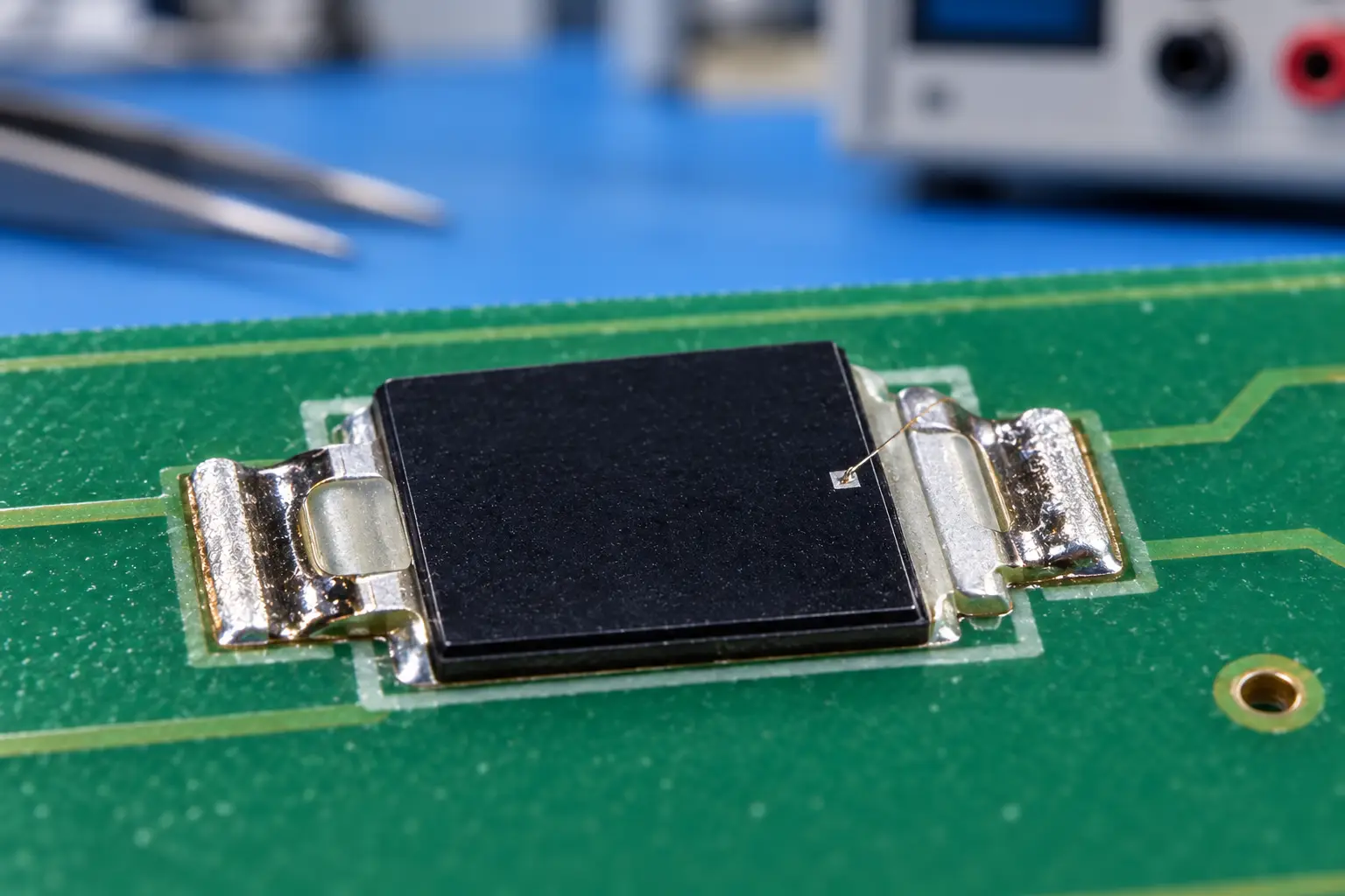
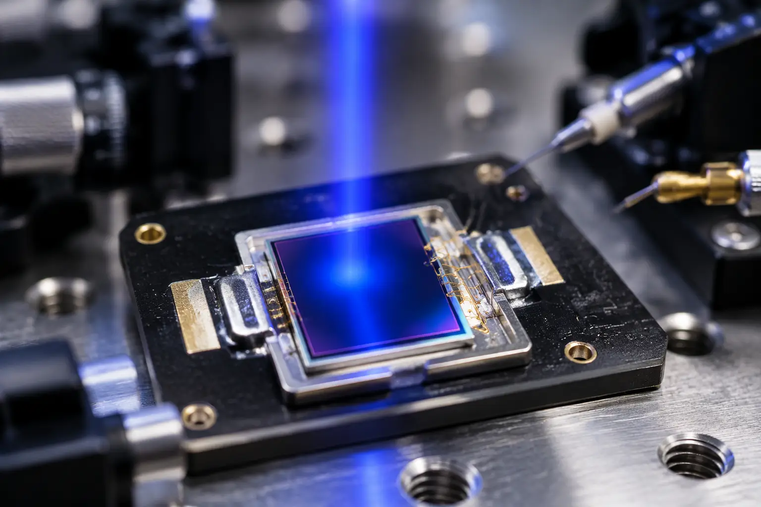
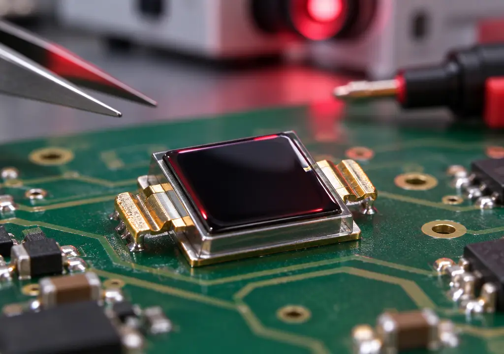
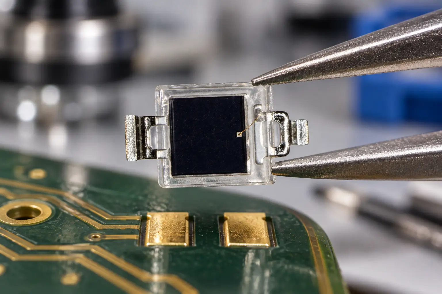
Modern sub-miniature sensors, such as the BeePhoton PDCP01-231 miniature series, feature a clear optical casting or mold resin designed to capture broad-spectrum light from 400 nm to 1100 nm, peaking across the near-infrared spectrum (850–940 nm).
Compared to older ceramic-based optical detectors, this molded small footprint detector keeps component height below 0.55 mm. This low-profile form factor is crucial when placing the miniature PIN photodiode 1.1×1.1 beneath 0.4 mm protective sapphire or polycarbonate covers in wearable wristbands and rings.
Core Electro-Optical Trade-Offs
When dealing with a miniature PIN photodiode 1.1×1.1, silicon physics forces you to juggle three interdependent parameters: junction capacitance, response speed, and dark current.
1. Junction Capacitance and Bandwidth Limits
The intrinsic (I) layer thickness determines both depletion width and junction capacitance (C_j). For a miniature PIN photodiode 1.1×1.1, the zero-bias capacitance hovers around 15 pF. That is remarkably low for an active area measuring roughly 0.36 mm², enabling clean frequency response without requiring massive reverse bias voltages.
The basic junction capacitance formula applies:
C_j = (epsilon_0 * epsilon_r * A) / W
Where:
- epsilon_0 = permittivity of free space (8.854 x 10^-12 F/m)
- epsilon_r = relative permittivity of silicon (~11.7)
- A = active junction area (m²)
- W = thickness of the depleted intrinsic layer (m)
Because the active area A in a miniature PIN photodiode 1.1×1.1 is inherently constrained, C_j stays low even at zero bias (VR = 0 V).
When interfacing the photodiode with a transimpedance amplifier (TIA), total input capacitance (C_in = C_j + C_amp_input + C_trace) sets the upper bound on the feedback loop’s closed-loop stability and bandwidth:
f_-3dB = sqrt( GBP / (2 * pi * R_f * C_in) )
Where:
- GBP = Gain Bandwidth Product of the operational amplifier (Hz)
- R_f = Feedback transimpedance resistor (Ohms)
- C_in = Total parasitic input node capacitance (Farads)
If you replace a legacy 3 mm photodiode having 80 pF capacitance with a miniature PIN photodiode 1.1×1.1 featuring just 15 pF, you immediately quadruple your stable bandwidth without touching the feedback resistor or burning extra battery current in your op-amp stage.
2. Dark Current and Noise Floor
Dark current (I_d) represents the leakage passing through the PIN junction when reverse-biased without incident light. In battery-powered instrumentation, I_d is the enemy because its shot noise sets the ultimate limit on minimum detectable signal:
I_shot = sqrt( 2 * q * (I_photo + I_d) * B )
Where:
- q = electron charge (1.602 x 10^-19 C)
- I_photo = photogenerated signal current (A)
- I_d = dark current (A)
- B = receiver noise bandwidth (Hz)
At 25°C and 5 V reverse bias, a high-grade miniature PIN photodiode 1.1×1.1 limits dark current to under 1 to 2 nA. But keep thermal runaway in mind: dark current doubles roughly every 8°C to 10°C rise in junction temperature, following the classic Shockley diode relationship documented across semiconductor standards like JEDEC JESD22.

Si PIN photodiode PDCP08 Series PDCP08-511
The PDCP08-511 is a high-performance Black Epoxy PIN Photodiode designed for precision infrared applications. Encased in a special black epoxy resin, this sensor effectively acts as a daylight filter, blocking visible light interference while maximizing sensitivity at 940nm. With a large 2.9×2.9mm active area and low dark current, it ensures reliable signal detection for optical switches and remote control systems, even in noisy ambient light environments.
Front-End Circuit Architectures: Photovoltaic vs. Photoconductive
A common point of disagreement among hardware designers is whether to reverse-bias a miniature PIN photodiode 1.1×1.1 in wearable devices.
Some engineers insist that every micro-photodiode must be reverse-biased to cut transit time and lower capacitance. On high-density boards, however, running a miniature PIN photodiode 1.1×1.1 at zero bias (photovoltaic mode) eliminates reverse dark-current drift, avoids thermal drift errors, and strips out an entire noisy bias-rail filtering network.
Here is how the two primary operating modes compare on the bench:
Photovoltaic Mode (Zero Bias Operation)
- Cathode Connection: Connected directly to the inverting input of the operational amplifier (virtual ground).
- Anode Connection: Connected directly to system analog ground (GND).
- Feedback Loop: Feedback resistor (R_f) placed in parallel with compensation capacitor (C_f) between op-amp output and inverting input.
- Key Benefit: Dark current drops to virtually zero picoamps. Thermal drift is heavily suppressed, making the miniature PIN photodiode 1.1×1.1 exceptionally stable for biometric pulses and low-light environmental monitoring.
Photoconductive Mode (Reverse Bias Operation)
- Cathode Connection: Connected to a positive clean bias supply rail (e.g., 3.3 V or 5 V).
- Anode Connection: Connected to the inverting input of the transimpedance amplifier.
- Feedback Loop: Similar R_f and C_f configuration sized for high-frequency phase margin.
- Key Benefit: Compresses the junction capacitance of the miniature PIN photodiode 1.1×1.1 from 15 pF down toward 5 pF. Accelerates carrier transit time for megahertz optical communications, rotary encoders, and fast optical interrupters.
If your application samples optical signals below 50 kHz—such as heart rate photoplethysmography (PPG) or slow paper-edge detection—photovoltaic mode using the miniature PIN photodiode 1.1×1.1 provides clean baselines and zero baseline dark-current offsets.
If you are designing high-speed time-of-flight, laser pulse synchronization, or optical encoders operating above 1 MHz, apply 3.3 V to 5 V of reverse bias to compress C_j from 15 pF down toward 5 pF. This drops carrier collection time into the low nanosecond regime.
Critical PCB Layout and Routing Rules
Working with a space-saving optical sensor measuring just 1.1 x 1.1 mm leaves zero margin for sloppy board routing. Common layout mistakes can degrade signal-to-noise ratios, create phantom optical reflections, or trigger mechanical solder skewing.
Minimizing Inverting Node Trace Capacitance
The junction trace running from the cathode or anode of your miniature PIN photodiode 1.1×1.1 to the inverting input of your TIA is the most sensitive trace on your board.
- Keep trace lengths under 3 mm. Place the amplifier input pin adjacent to the detector pad.
- Never run high-speed digital clocks, SPI buses, or switching boost converter traces parallel to or directly beneath this node.
- Void internal ground and power planes directly beneath the photodiode anode/cathode pads and the inverting input pin of the amplifier. Solid copper planes beneath these pads introduce 1 to 3 pF of stray parasitic capacitance, degrading phase margin and causing peaking in the optical frequency response.
Guard Rings for Sub-Nanoamp Leakage
When tracking sub-nanoamp photodiode currents, board surface currents can easily mask the actual light signal. Contaminants, solder flux residue, and ambient humidity create surface leakage resistance paths as low as 100 Megohms, which can overwhelm your signal path.
Guard Ring Geometry Implementation:
- Form an unbroken ring of surface copper surrounding the delicate trace connecting the miniature PIN photodiode 1.1×1.1 to the TIA inverting input pad.
- In single-supply, zero-bias setups, tie this guard trace directly to ground.
- In dual-supply or non-zero reference designs, drive the guard ring with a buffered trace equal to the non-inverting terminal potential.
- Do not cover the guard ring copper with soldermask. Leaving the guard copper bare ensures surface contamination currents intercept the guard boundary instead of migrating into your photodiode pad.
For detailed engineering recommendations on guard ring geometry, parasitic capacitance reduction, and board-level shielding, consult the Analog Devices High-Speed Printed Circuit Board Layout Guide alongside the Texas Instruments Transimpedance Design Guide.
Comparing the Miniature PIN Photodiode 1.1×1.1 Against Alternative Form Factors
Optical component selection always balances package dimensions against responsive surface area. The following comparison illustrates where the miniature PIN photodiode 1.1×1.1 fits within the broader BeePhoton Silicon PIN Photodiode product line.
| Sensor Model | Package Dimensions (mm) | Active Area (mm²) | Typ. Capacitance (VR = 0V) | Typical Package Construction | Primary Target Applications |
|---|---|---|---|---|---|
| Miniature PIN Photodiode 1.1×1.1 (PDCP01-231) | 1.1 x 1.1 x 0.5 | ~0.36 | 15 pF | Micro clear epoxy / mold SMT | Smart rings, earables, micro slotted switches |
| PDCP08-511 | 5.0 x 4.0 x 1.2 | ~7.5 | ~70 pF | Daylight filter black mold | IR remote controls, curtain safety barriers |
| PDCP08-502 | 2.9 x 2.8 x 1.0 | ~2.0 | ~35 pF | Compact clear top-view SMT | Industrial optical encoders, pulse oximetry |
| PDCP08-501 | 3.0 x 2.0 x 1.1 | ~1.5 | ~25 pF | Mid-sized SMT package | Edge detection, optical tachometers |
While models like the PDCP08-511 maximize capture area for long-range IR links, their 5.0 x 4.0 mm footprint simply won’t fit into space-critical assemblies.
Likewise, the PDCP08-502 and PDCP08-501 serve mid-sized optoelectronic instruments, but cannot match the pack-level layout density offered by the miniature PIN photodiode 1.1×1.1.
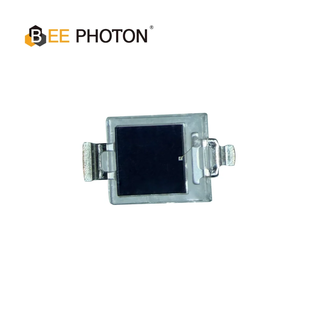
Si PIN photodiode PDCP08 Series PDCP08-501
High-Performance Detection: The PDCP08-501 is a high-speed Silicon PIN Photodiode with a transparent window.
Key Specs: Featuring a 2.9×2.9mm active area, this PIN photodiode offers low dark current and high responsivity, making it an ideal sensor for general optical switches and light detection systems.
Real-World Applications
Where does this tiny optical detector deliver the greatest impact? Two engineering case studies highlight its distinct advantages.
Case 1: Ultra-Thin Smart Ring Optical Array
A developer of high-density biometric wearables needed to measure heart rate (PPG) and blood oxygen saturation (SpO_2) within an inner ring circumference of under 18 mm. The available board width measured only 2.4 mm.
The mechanical and optical stack was assembled in the following sequence:
- Top Protective Layer: Biocompatible, transparent resin outer window contoured to the finger tissue.
- Optical Isolation Layer: Dual laser-cut black silicone baffles blocking direct lateral radiation paths.
- Component Placement Layer: A central miniature PIN photodiode 1.1×1.1 flanked on one side by a 525 nm green micro-LED and on the other by a 940 nm infrared micro-LED.
- Base Substrate: A high-density 4-layer polyimide rigid-flex circuit board carrying analog traces to an ultra-low-power microcontroller.
The engineering challenges:
- Conventional 0805 or 1206 photodiode packages exceeded the flex-PCB’s available width once clearance rules and passive components were included.
- Direct optical crosstalk from the flanking green (525 nm) and infrared (940 nm) LEDs risked blinding the optical detector through internal reflection within the outer acrylic cover.
The implementation:
- Using two units of the miniature PIN photodiode 1.1×1.1, the engineering team placed the detectors along the center axis, flanking them with miniature LEDs separated by physical opaque baffles.
- The combined low capacitance of 15 pF allowed rapid 50-microsecond sampling pulses without settling-time distortion, lowering total LED driver power consumption by 32%.
- The compact 1.1 x 1.1 mm footprint left adequate clearance for an integrated physical optical barrier, keeping baseline optical crosstalk below 0.05% of full-scale transimpedance output.
Case 2: Micro Slotted Optical Interrupter for Compact Mechanisms
In precision linear stages, miniature drone gimbals, and automated medical pipettes, standard 3 mm slotted optical interrupter switches add too much bulk.
Using a discrete emitter paired with a miniature PIN photodiode 1.1×1.1, engineers constructed an ultra-compact slotted interrupter according to these sub-assembly parameters:
| Assembly Element | Chosen Component / Dimension | Operational Function |
|---|---|---|
| Infrared Emitter | 0402 package NIR LED (940 nm) | Emits narrow forward beam across the motion channel. |
| Air Gap Throat Width | 1.2 mm physical channel | Allows clearance for a moving code-wheel flag or shutter vane. |
| Aperture Slit | 0.25 mm laser-drilled brass mask | Sharpens beam transition edge for sub-micron position repeatability. |
| Detector Stage | Miniature PIN Photodiode 1.1×1.1 | Converts incoming unblocked NIR photons into microamp pulses. |
With an active area of roughly 0.36 mm², the miniature PIN photodiode 1.1×1.1 couples efficiently with a 0.25 mm micro-aperture. The quick carrier transit time provides clean, jitter-free logic transitions even when detecting high-speed rotor blades spinning past 25,000 RPM.
Assembly, Soldering, and SMT Processing
Working with sub-miniature optoelectronic components requires close attention to standard pick-and-place assembly techniques, as detailed in established Surface-Mount Technology Standards and related footprint practices.
Stencil Aperture and Solder Bridging
Because the pad pitch of a miniature PIN photodiode 1.1×1.1 is narrow, apply a 10% to 15% area reduction on the solder paste stencil. Using standard 1:1 apertures often causes solder paste to squeeze across the center gap, resulting in microscopic solder bridges beneath the component body.
Avoid homebrew footprint pads. Adhere strictly to the land pattern dimensions provided by the component manufacturer. If your solder pads extend unevenly beyond the package perimeter, surface tension during reflow will tilt the sensor, skewing its optical axis off-center.
Cleaning and Flux Traps
Due to the low clearance of 0.1 mm between the bottom of the miniature PIN photodiode 1.1×1.1 package and the board surface, flux residue can easily get trapped underneath.
Standard “no-clean” rosin flux can leave behind a conductive ionic film that generates picoamp-level leakage paths under high ambient humidity. In high-precision optical front-ends, use an automated ultrasonic isopropyl alcohol (IPA) wash or deionized water wash cycle to keep the sensor base clean.
Optical Packaging, Windows, and Crosstalk Suppression
A high-performance miniature PIN photodiode 1.1×1.1 cannot overcome poor optomechanical housing design. In compact assemblies, optical crosstalk—where emitter light couples directly into the photodiode through protective window layers—remains the primary source of signal degradation.
The following optical design rules differentiate failed prototypes from production-ready units:
- Separated Optical Windows: Never mount both the emitter LED and the miniature PIN photodiode 1.1×1.1 beneath a continuous, unpartitioned sheet of clear glass or acrylic. The plastic cover acts as an internal light pipe, funneling direct emitter rays straight into the detector.
- Opaque Partition Baffles: Run a physical, light-blocking rib made of black polyoxymethylene (POM) or opaque silicone from the PCB surface all the way flush against the bottom surface of the window.
- Absorptive Internal Coatings: Paint internal plastic surfaces with matte black light-absorbing coatings or specify micro-grooved textures to kill internal glancing reflections.
- Wavelength-Selective Filtering: In high ambient light environments, place a thin narrowband optical bandpass coating over the miniature PIN photodiode 1.1×1.1 window. While silicon responds from 400 nm to 1100 nm, bandpass filtering ensures the sensor registers only your target emitter pulses.

Si PIN photodiode PDCP08 Series PDCP08-502
The PDCP08-502 is a high-response 2.9×2.8mm Silicon PIN Photodiode designed for precision photoelectric applications. Featuring low junction capacitance, low dark current, and a wide spectral range (340-1100nm), it is the ideal component for optical switches and compact sensing modules requiring stable and fast signal output.
Frequently Asked Questions
Can the miniature PIN photodiode 1.1×1.1 detect visible light, or is it restricted to infrared?
The silicon substrate responds to photon energies from approximately 400 nm up to 1100 nm. Although its peak responsivity sits in the near-infrared band (850–940 nm at ~0.55 A/W), it can easily detect visible light (such as 525 nm green LEDs) at a responsivity of roughly 0.20 to 0.30 A/W. If your application requires strict visible-light rejection, specify an optical filter or opt for clear epoxy variants shielded by a secondary filter window.
What is the maximum reflow soldering temperature for the miniature PIN photodiode 1.1×1.1?
Standard lead-free reflow profiles apply, with a peak temperature (T_p) of 260°C for no more than 10 seconds, in accordance with IPC/JEDEC J-STD-020 standards. Avoid extended thermal soaking above 200°C, which can degrade the optical transmittance of the clear encapsulation resin.
How does changing reverse bias affect the capacitance of a miniature PIN photodiode 1.1×1.1?
At zero bias (VR = 0 V), the internal capacitance is typically 15 pF. Increasing reverse bias expands the depletion region, lowering junction capacitance down to approximately 5–7 pF at VR = 5 V. For low-frequency biometric monitoring, the 15 pF zero-bias capacitance is already small enough to run without reverse bias, saving battery life and avoiding dark current drift.
How should the miniature PIN photodiode 1.1×1.1 be handled during automated SMT pick-and-place?
Use a pick nozzle with an outer diameter no larger than 0.7 mm, equipped with a compliant rubber or polyimide tip. Avoid hard stainless-steel pick tools that can scratch, crack, or indent the clear optical casting surface directly above the active silicon area.
Conclusion & Next Steps
When space constraints rule out traditional optical packaging, the miniature PIN photodiode 1.1×1.1 delivers the right balance of a compact 1.1 x 1.1 mm footprint, low 15 pF junction capacitance, and reliable sub-nanosecond response.
Whether you are routing a micro wearable flex-circuit, upgrading an optical encoder array, or developing a custom slotted switch, paying close attention to board layout parasitics, guard rings, and optical isolation ensures your design meets its performance targets.
If you are developing an ultra-compact optoelectronic project, contact the engineering team at BeePhoton through their Direct Contact Page or by email at info@photo-detector.com.
Request technical datasheets, CAD footprints, and bench evaluation samples for the PDCP01-231 series to test the miniature PIN photodiode 1.1×1.1 on your prototype boards today.