If you have ever spent three weeks trying to align an external plastic plano-convex lens with a tiny surface-mount detector inside an IP67 aluminum housing, you know the pain. You run optical ray traces in Zemax, everything looks flawless on screen, and then manufacturing builds the first fifty prototypes. Suddenly, half your optical budget evaporates because tolerance stack-ups on the mechanical bracket shifted the focal point by barely 0.4 millimeters.
That headache is why many experienced hardware teams turn back to an integrated approach: the through-hole photodiode with lens.
Integrating optics straight onto a leadframe package might sound old-school compared to pick-and-place surface-mount diodes. But when you are designing perimeter tripwires, industrial safety curtains, or outdoor rangefinders measuring beyond ten meters, optical physics does not care about component trends. A dedicated through-hole photodiode with lens packs optical gain, environmental shielding, and narrow directional focus right into the component body. It eliminates intermediate air-glass interfaces, drops part counts, and dramatically tightens your system signal-to-noise ratio.
Let us walk through how these devices behave in real circuits, analyze the optical mechanics behind molded package profiles, and look at why using a through-hole photodiode with lens saves you significant factory calibration hours.
The Optical Geometry: Why Integrated Lenses Beat External Glass
Every optical receiver system fights the same fundamental equation: collecting enough signal photons while keeping out ambient background noise. When building a long-range optical barrier or light curtain, an engineer typically starts with a standard flat-window silicon detector. You quickly realize you need more axial gain, so you add a separate optical barrel with a molded acrylic lens.
That approach immediately introduces three engineering liabilities:
- Fresnel Reflection Losses: Each new boundary between air and plastic or glass reflects around 4% of incident photons (governed by Fresnel formulas based on refractive index mismatches). With an external lens and an air gap before your detector window, you drop 8% to 15% of your light before it ever touches silicon.
- Tolerance Stack-Up: The lens barrel has a tolerance, the PCB mounting holes have a tolerance, and the diode package placement has a tolerance. A 1-degree mechanical tilt can drop received power on a small active area by more than 6 dB.
- Moisture and Condensation: Air gaps invite humidity. Condensation inside an optical cavity scatters your collimated beam, triggering false alarms in outdoor laser tripwires.
External Lens Configuration (Multi-Interface Path):
Source Beam -> Air Barrier -> External Lens Surface -> Internal Air Gap (Moisture Risk & 8% to 15% Fresnel Loss) -> Planar Detector Window -> Silicon DieIntegrated Lensed Configuration (Direct Interface Path):
Source Beam -> Cast Optical Epoxy Dome -> Solid Polymer Interface (Index Match n = 1.52) -> Direct Silicon Die
A properly engineered through-hole photodiode with lens sidesteps these problems entirely. The casting epoxy acts as both the encapsulant and the primary optical surface. Light travels directly from the outer curved boundary into an optical polymer having a refractive index typically between 1.51 and 1.54, striking the silicon die without passing through any unsealed internal air gaps.
Practical bench tip: When evaluating optoelectronic components for industrial equipment, remember that every mechanical fastener or alignment clip you eliminate from an optical assembly cuts your long-term field failure rates due to vibration creep.
According to technical documentation on radiometry and photodetector operation from NIST, optical efficiency relies heavily on minimizing unwanted scatter and maximizing the collection area. By curing an optical-grade domed lens directly over the silicon die, the active collection area effectively multiplies via refraction, turning a modest 0.8 mm² die inside a through-hole photodiode with lens into an optical receiver with the collection power of a much larger sensor.
Axial Sensitivity and Field of View (FOV) Mechanics
The core benefit of picking a through-hole photodiode with lens is axial optical gain. When light hits a spherical or cylindrical dome, Snell’s law bends the incoming rays toward the central normal axis.
Understanding Numerical Aperture and Acceptance Angles
The acceptance angle, often rated as the half-angle (theta 1/2), tells you where the detector responsivity drops to 50% of its peak on-axis value. A bare planar photodiode has a broad Lambertian profile with an acceptance angle approaching +/- 60 degrees. That is great for ambient light sensors on a dashboard, but disastrous for a 30-meter optical perimeter barrier exposed to bright sunlight.
A through-hole photodiode with lens constricts that acceptance cone. By tightening the beam angle down to +/- 10 degrees, +/- 15 degrees, or +/- 20 degrees, you transform the device into a true narrow angle photodetector.
To calculate the spatial solid angle (Omega) of your receiver field of view:
Omega = 2 * pi * (1 – cos(theta_half))
If your acceptance half-angle (theta_half) is 60 degrees (typical planar sensor):
Omega = 2 * pi * (1 – cos(60)) = 2 * pi * (1 – 0.5) = pi steradians (~3.14 sr)
If you switch to a narrow angle through-hole photodiode with lens where theta_half is 12 degrees:
Omega = 2 * pi * (1 – cos(12)) = 2 * pi * (1 – 0.9781) = 0.137 steradians
Look at that difference: 3.14 sr down to 0.137 sr. By restricting the solid angle by a factor of 22, the through-hole photodiode with lens blocks approximately 95% of off-axis diffuse ambient sunlight and stray industrial factory reflections from entering the detector.

Si PIN photodiode PDCP08 Series PDCP08-511
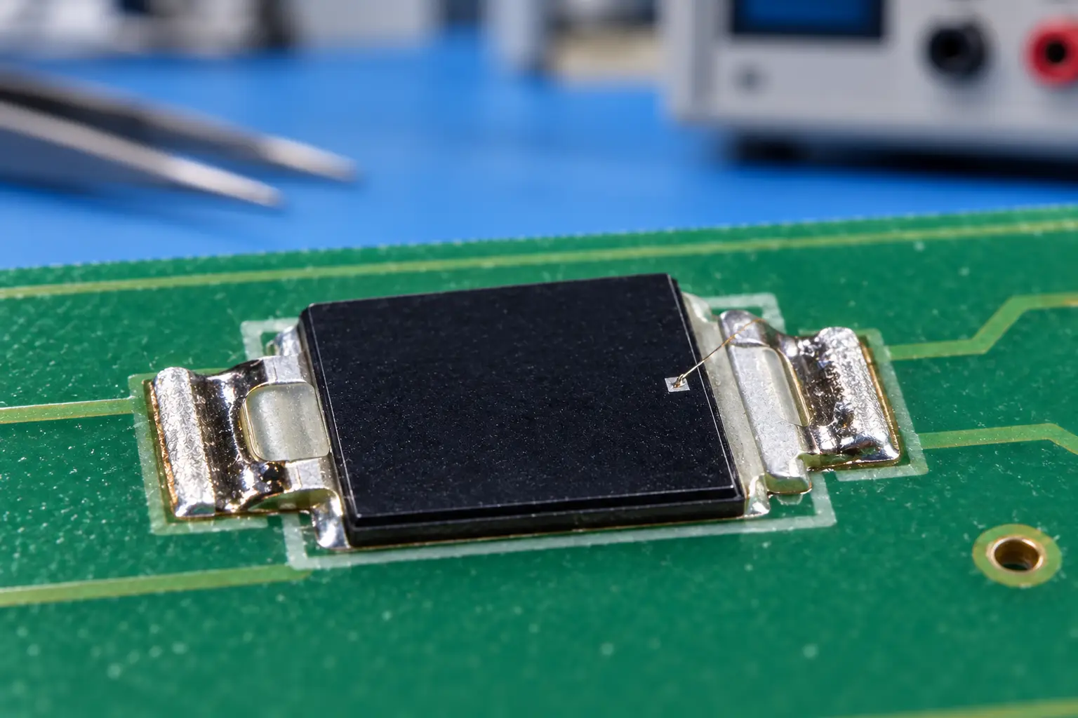
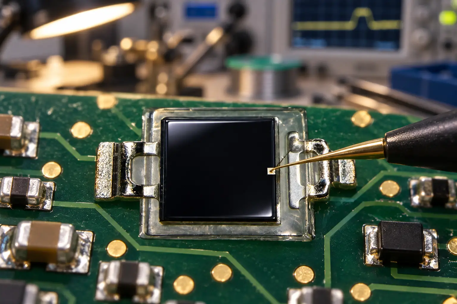
The PDCP08-511 is a high-performance Black Epoxy PIN Photodiode designed for precision infrared applications. Encased in a special black epoxy resin, this sensor effectively acts as a daylight filter, blocking visible light interference while maximizing sensitivity at 940nm. With a large 2.9×2.9mm active area and low dark current, it ensures reliable signal detection for optical switches and remote control systems, even in noisy ambient light environments.
Comparing Package Optical Performance
| Parameter | Standard Flat TO-92 / SMT | Cylindrical Lens DIP | Domed Round Lens DIP |
|---|---|---|---|
| Typical Half-Angle (theta 1/2) | +/- 60 deg to +/- 75 deg | +/- 15 deg (Axis A) / +/- 40 deg (Axis B) | +/- 10 deg to +/- 20 deg |
| Relative On-Axis Responsivity | 1.0x (Baseline) | 2.5x to 3.5x | 3.0x to 5.5x |
| Alignment Tolerance | Very forgiving | Sensitive along curve, wide along slot | Sensitive in both X and Y axes |
| External Collimator Needed? | Yes, for long ranges | No, in most slotted/line applications | No, for point-to-point beams |
| Sunlight Rejection Ability | Poor (Requires baffles) | Moderate to High | High (Narrow spatial filter) |
When you review the specs for a directional through-hole photodiode with lens, you will notice that the on-axis current generation jumps significantly compared to its bare die rating. If your unlensed silicon yields a short-circuit current of 15 microamps under a given test source, the exact same die inside a through-hole photodiode with lens can produce 45 to 75 microamps on-axis.
DIP Cylindrical Lens Photodiode vs. Spherical Domed Packaging
Not every long-range sensor requires a circular pinpoint beam. In fact, one of the most frustrating aspects of building industrial safety barriers or elevator door detectors is dealing with vertical alignment sag over long distances.
This is where picking between a spherical dome and a DIP cylindrical lens photodiode becomes critical.
Spherical Domed Lenses: Best for Pinpoint Point-to-Point Links
A standard round through-hole photodiode with lens features a symmetrical spherical or parabolic dome. This focuses incoming light uniformly along both the X and Y axes.
- Pros: Maximum axial gain; concentrates the highest optical flux density onto the silicon junction.
- Cons: If your transmitter pole shifts slightly due to thermal expansion or foundation settling, the signal drops out completely.
Cylindrical Lens DIP: Asymmetric Field of View
A DIP cylindrical lens photodiode uses an extruded cylindrical radius on top of the package. It compresses the field of view sharply in one dimension while maintaining a broader acceptance angle in the other.
- Horizontal plane: Tight beam acceptance (for example, +/- 12 degrees) to reject interference from neighboring machines or adjacent light barriers.
- Vertical plane: Generous beam acceptance (for example, +/- 35 degrees) so your transmitter and receiver do not lose optical coupling when mounting brackets expand or vibrate under heavy plant operation.
For engineers working with automated sorting lines or multi-beam safety arrays meeting standards like IEC 61496 for electro-sensitive protective equipment, utilizing an asymmetric directional optical sensor saves dozens of hours in field alignment. You get horizontal optical rejection without needing a jeweler’s touch to line up the vertical height.
For specialized industrial designs requiring clean NIR filtering, teams often implement filtered components like the PDCP08-511 black epoxy PIN photodiode, which blocks visible ambient daylight while letting the 850nm to 940nm emitter signals pass right into the junction.
Signal-to-Noise Ratio (SNR) in Long-Distance Applications
Let us get into the circuitry math. Optical design is useless if your front-end transimpedance amplifier (TIA) cannot distinguish between signal photocurrent and dark current noise.
When your transmitter is 20 meters away, optical irradiance drops according to the inverse-square law:
E_e = (I_e * tau_atm) / d^2
Where:
- E_e is the irradiance at the receiver plane (Watts per square meter)
- I_e is the radiant intensity of the emitter LED or laser diode (Watts per steradian)
- tau_atm is the atmospheric transmission coefficient (typically 0.90 to 0.98 in clean air)
- d is the distance between emitter and receiver (meters)
At 20 meters, d^2 is 400. That means your optical power density at the receiver is 1/400th of what it was at 1 meter.
The Photocurrent Generation Equation
The generated photocurrent (I_ph) in your detector is:
I_ph = P_rx * R_lambda
Where P_rx is the total optical power collected by the active optical aperture and R_lambda is the spectral responsivity in Amperes per Watt (A/W) at your operational wavelength. For high-speed silicon at 850nm to 905nm, responsivity is typically between 0.55 A/W and 0.65 A/W. Fundamental responsivity behavior across silicon substrates is well documented on Wikipedia’s photodiode physics page.
Now compare what happens when you use an ordinary flat photodiode versus a through-hole photodiode with lens:
Optical Power Collection Comparison:
Planar Diode: P_rx_planar = E_e * A_die
Through-Hole Photodiode with Lens: P_rx_lensed = E_e * A_die * Optical_Gain_Factor
The Optical_Gain_Factor of a quality molded epoxy through-hole photodiode with lens generally runs between 2.5 and 5.0.
Impact on Front-End Noise
Why not just take the tiny signal from a flat photodiode and turn up the feedback resistor (R_f) on your operational amplifier? Because physics pushes back via Johnson-Nyquist noise and shot noise.
The total noise current (I_noise) in a basic transimpedance amplifier is calculated as:
I_noise = sqrt( (2 * q * (I_ph + I_dark + I_ambient) * BW) + (4 * k_B * T * BW / R_f) )
Where:
- q is the electron charge (1.602 x 10^-19 Coulombs)
- I_dark is the photodiode dark current
- I_ambient is the DC photocurrent caused by room lights or sunlight
- BW is the amplifier bandwidth (Hz)
- k_B is Boltzmann’s constant (1.38 x 10^-23 J/K)
- T is absolute temperature in Kelvin
- R_f is the transimpedance feedback resistor value (Ohms)
If you use a flat-window sensor with a wide field of view, I_ambient is huge because the diode drinks in all background sunlight and overhead fluorescent flicker. That massive I_ambient blows up your shot noise under the radical sign.
When you swap that out for a through-hole photodiode with lens:
- I_ambient drops drastically because the narrow spatial acceptance angle physically rejects out-of-beam ambient photons.
- I_ph (your desired signal) jumps because the lens dome focuses more incident emitter energy onto the die.
- Your signal increases linearly, while shot noise only increases with the square root of current.
The net result? A massive jump in overall system SNR without requiring complex multi-stage optical filters or expensive lock-in amplifier stages. Deploying a through-hole photodiode with lens simply gives your analog front-end cleaner raw signals to work with.

Si PIN photodiode PDCP08 Series PDCP08-502
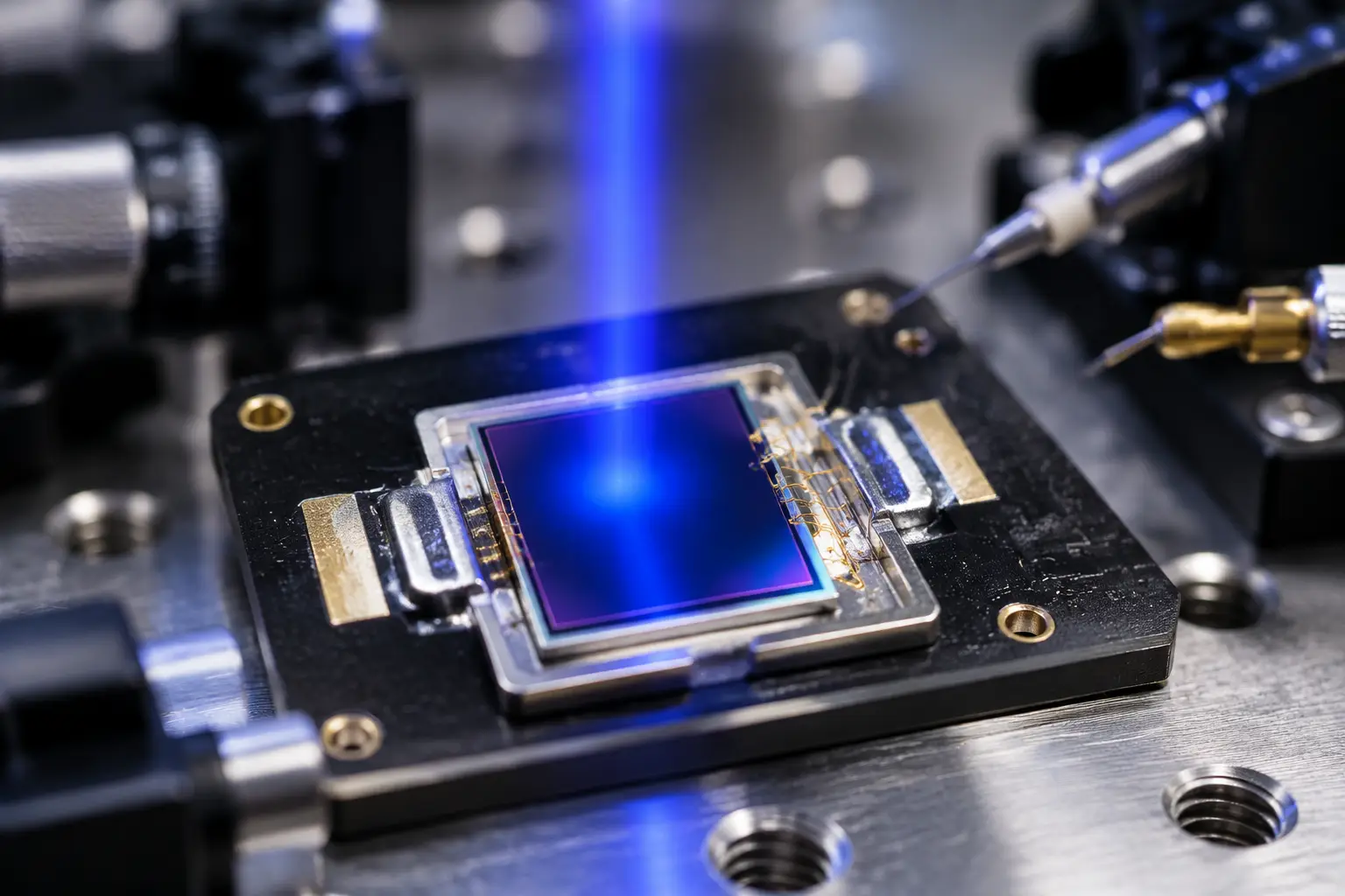
The PDCP08-502 is a high-response 2.9×2.8mm Silicon PIN Photodiode designed for precision photoelectric applications. Featuring low junction capacitance, low dark current, and a wide spectral range (340-1100nm), it is the ideal component for optical switches and compact sensing modules requiring stable and fast signal output.
Real-World Case Study: Outdoor Light Curtain False Triggers
A commercial logistics equipment manufacturer was experiencing intermittent signal loss on an automated cargo scanning gantry. The system used an array of 32 emitter-detector pairs spaced 8 meters apart across an outdoor loading lane.
The Problem
The initial design used compact surface-mount PIN photodiodes mounted flush against clear polycarbonate protective windows on the receiver pillar. During early morning and late afternoon hours, when the sun dipped low on the horizon, direct solar glare flooded the planar photodiodes.
Even though the emitter modulated at 40 kHz, the background solar irradiance was driving the transimpedance amplifiers into rail-to-rail saturation. The DC photocurrent from the sun was over 800 microamps, completely washing out the small 1.2 microamp AC pulse generated by the pulsed infrared laser diodes.
The team attempted to remedy this by 3D-printing individual plastic mechanical snoots (egg-crate baffles) in front of each SMD sensor. While this reduced solar saturation, it increased bill-of-materials costs, complicated the weatherproofing gasket, and made manual factory assembly an alignment nightmare.
The Solution
The engineering team switched from surface-mount detectors to a dedicated through-hole photodiode with lens array, specifically selecting a package featuring high-transmittance optical epoxy with an integrated visible-light-blocking daylight filter.
Architecture Transition:
Previous Layout: Polycarbonate Window -> Stray Sunlight Enters Wide Angle (+/-65 deg) -> SMD Flat Diode -> TIA Rail Saturation
Upgraded Layout: Polycarbonate Window -> Off-Axis Sunlight Rejected (+/-15 deg) -> Through-Hole Photodiode with Lens -> Clean 2.6 uA Signal
By substituting the planar diodes with a high-gain through-hole photodiode with lens featuring a narrow +/- 15 degree acceptance cone:
- Ambient solar saturation current dropped from 800 microamps down to under 38 microamps.
- The on-axis signal from the 8-meter pulsed emitter doubled from 1.2 microamps to 2.6 microamps due to the integrated lens gain of the through-hole photodiode with lens.
- The 3D-printed baffles were scrapped entirely, eliminating two injected-molded sub-brackets and trimming assembly labor by 4 minutes per receiver pillar.
For compact systems where board space is tight but engineers still need high responsivity, selecting matched geometry detectors like the PDCP08-502 2.9×2.8mm silicon PIN photodiode or the PDCP08-501 silicon PIN photodiode gives layout flexibility while retaining high sensitivity.
If your team is designing custom detection channels, you can review our full engineering lineup directly through the BeePhoton homepage.
Assembly and Production Realities: Through-Hole vs. Surface-Mount
Let us address the elephant in the room: board assembly. SMT components run through high-speed pick-and-place machines at twenty thousand parts per hour. Why would an engineer deliberately choose a through-hole photodiode with lens in a modern hardware project?
The answer comes down to mechanical structural integrity and optical axis orientation.
Wave Soldering vs. Reflow Temperatures
Surface-mount plastic photodetectors must endure reflow oven temperatures exceeding 250 degrees Celsius. While modern optical polymers can survive lead-free reflow profiles, the high heat stresses the junction interface and can induce subtle micro-cracking or yellowing in the optical epoxy. That degrades transmission efficiency over time.
A through-hole photodiode with lens uses classic DIP leads. The sensitive optical dome stays on the top side of the PCB, safely isolated from direct thermal shock while the leads touch wave-soldering fingers or selective soldering pots beneath the board. The optical dome on the through-hole photodiode with lens maintains crystal-clear clarity with zero heat-induced haze.
Right-Angle Bending and Optical Boresighting
In most long-range sensors, your beam travels parallel to the PCB surface rather than shooting down perpendicular into the board.
With an SMT photodiode, achieving horizontal orientation requires either:
- A secondary daughterboard mounted at a 90-degree angle (costly, adds connector reliability concerns).
- An edge-mount “side-looker” SMT package (notoriously prone to floating or tilting during solder reflow).
With a through-hole photodiode with lens, you simply order the component with pre-formed right-angle leads—or form them with a standard lead-forming jig. The rigid copper-alloy leads anchor the component securely into the through-plated PCB barrels. Once soldered, the optical center axis of your through-hole photodiode with lens stays locked in place, even under heavy industrial mechanical shock.
For complex installations requiring exact part cross-referencing—such as replacing older or obsolete components like the PDCP08-403 series—having a leaded through-hole photodiode with lens that can be physically adjusted during optical calibration is a lifesaver.
Optical Alignment Techniques in Production
While a through-hole photodiode with lens provides built-in gain, its narrower acceptance angle means you cannot just solder it onto a board haphazardly and expect your beam to line up. A 2-degree mounting tilt over a 25-meter sensing distance shifts your beam footprint center by nearly a meter:
Delta_y = d * tan(theta_tilt)
Delta_y = 25m * tan(2 deg) = 25m * 0.0349 = 0.87 meters
If your beam waist is only 0.5 meters wide at that range, a 2-degree assembly tilt will cause your through-hole photodiode with lens to miss the optical cone entirely!
Here is how experienced manufacturing lines handle alignment when using a through-hole photodiode with lens:
1. Mechanical Alignment Collars
Do not rely on your line operators’ eyes to position the photodiode straight. Design matching plastic standoffs or PCB guide bosses into your housing. When the through-hole photodiode with lens is inserted through the PCB, the epoxy shoulder drops into a molded cavity that locks the optical axis true to the enclosure mounting datum.
2. Laser Diode Fixturing During Soldering
For high-precision optoelectronic devices, assemble the boards using an active alignment fixture. The through-hole photodiode with lens is slipped into place, a low-cost collimated alignment laser fires down the target axis onto the lens dome, and the operator confirms peak output current on a digital readout before activating the selective-soldering foot pedal.
3. Lead Forming Jigs
Never bend lead wires by hand with needle-nose pliers right against the package base. The mechanical stress will shear the internal bond wire away from the silicon die or fracture the epoxy hermetic seal. Always use a proper bending tool that supports the lead wire between the package body and the bend radius. Keep the bend line of your through-hole photodiode with lens at least 2.5 mm away from the epoxy casting base.
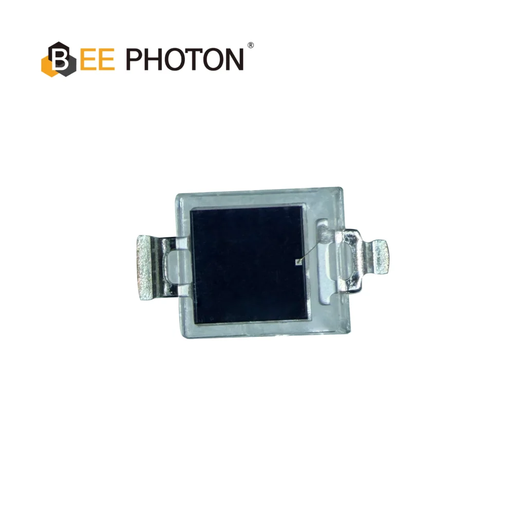
Si PIN photodiode PDCP08 Series PDCP08-501
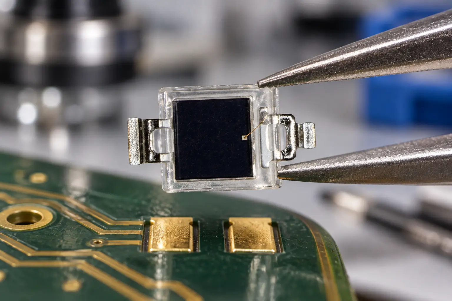
High-Performance Detection: The PDCP08-501 is a high-speed Silicon PIN Photodiode with a transparent window.
Key Specs: Featuring a 2.9×2.9mm active area, this PIN photodiode offers low dark current and high responsivity, making it an ideal sensor for general optical switches and light detection systems.
Common Pitfalls When Implementing Lensed Detectors
Even the best through-hole photodiode with lens can underperform if the surrounding system architecture is flawed. Here are three common design errors observed across optical engineering teams:
Ignoring Internal Reflections from Front Glazing
Many engineers place an external flat protective window in front of their through-hole photodiode with lens to keep dust out of the enclosure. If you position the flat window too close to the curved epoxy dome of the through-hole photodiode with lens, stray light can bounce between the convex surface and the inner face of the flat glass, setting up parasitic reflections that destroy directional sensitivity.
- The Fix: Maintain an optical clearance gap of at least 3 times the dome radius, or angle the protective external window by 3 to 5 degrees to reflect specular returns harmlessly out of the optical path.
Saturating the TIA with Modulated Optical Harmonics
Because a through-hole photodiode with lens gathers significantly more on-axis light than a flat sensor, ensure your transimpedance amplifier does not saturate when the emitter and receiver are brought close together. An automated guided vehicle (AGV) sensor might need to work at 20 meters, but it also has to dock at 0.5 meters.
- The Fix: Implement a logarithmic amplifier topology, or incorporate an active automatic gain control (AGC) loop that steps down the amplifier feedback resistance when strong signals hit the through-hole photodiode with lens.
Assuming Optical Epoxy Lasts Forever Under Intense UV
If your equipment operates outdoors in harsh climates, standard optoelectronic packaging polymers can degrade from intense solar ultraviolet radiation over five to ten years.
- The Fix: Specify a through-hole photodiode with lens cast from UV-stabilized optical-grade epoxy resins, or verify that your outer enclosure window includes a durable UV-blocking substrate coating (such as standard optical borosilicate or coated polycarbonate).
Selecting the Right Component for Your Sensor Architecture
When specifying a through-hole photodiode with lens for your bill of materials, systematically check off these electrical and optical parameters:
- Wavelength Matching: Match your detector peak sensitivity band to your emitter. Silicon naturally peaks around 850nm to 920nm. If you are using visible 650nm red lasers, verify that the epoxy formulation on your through-hole photodiode with lens does not have heavy visible absorption characteristics.
- Speed vs. Active Area: Optical lenses let you keep the silicon junction small (for instance, 1 mm² or less) while gathering light like a 5 mm² die. A smaller die yields lower junction capacitance. If your signal requires megahertz-level modulation or rapid nanosecond pulse detection, pairing a small die with a high-magnification through-hole photodiode with lens provides both high bandwidth and high responsivity.
- Lead Spacing and Footprint: Standard DIP lead spacing is 2.54 mm (0.1 inch). Confirm whether your PCB layout uses standard pitch or requires offset leads for polarized orientation keys when placing the through-hole photodiode with lens.
If you have specific optical isolation or mechanical mounting requirements, reach out to our optoelectronic engineering group through the BeePhoton Contact Page. We help teams customize package styles, epoxy tints, and acceptance angles to match challenging sensor layouts with the right through-hole photodiode with lens.
Frequently Asked Questions
What makes a through-hole photodiode with lens better than an SMT sensor with an external lens?
A through-hole photodiode with lens eliminates the air-to-plastic transition between the lens and the die, reducing Fresnel reflection losses by roughly 8% to 15%. It also removes mechanical tolerance stack-ups caused by mounting separate optical barrels, simplifies assembly down to a single solderable component, and keeps dust or moisture from collecting inside the optical path.
How does the lens affect the photodiode junction capacitance and response speed?
The lens itself adds zero capacitance because it is simply optical epoxy sitting outside the active junction. However, choosing a through-hole photodiode with lens allows you to specify a photodiode with a much smaller active silicon area while still collecting sufficient optical power. Because junction capacitance scales directly with die area, choosing a through-hole photodiode with lens lets you achieve much faster rise times and higher operational bandwidth than would be possible using a large, unlensed silicon die.
Can a through-hole photodiode with lens work in outdoor sunlight?
Yes, particularly when you select a through-hole photodiode with lens cast from visible-light-blocking black epoxy or incorporate an infrared daylight filter. The narrow spatial acceptance angle of a through-hole photodiode with lens rejects the vast majority of off-axis diffuse solar radiation, preventing your receiver amplifier circuit from being driven into saturation.
What is the difference between a spherical lens and a cylindrical lens DIP photodiode?
A spherical dome through-hole photodiode with lens focuses light symmetrically along both axes, yielding a narrow, circular acceptance cone with maximum axial gain. A DIP cylindrical lens through-hole photodiode with lens focuses light sharply along only one axis (for instance, horizontally), while maintaining a broad acceptance angle along the vertical axis. This makes cylindrical models ideal for light curtains and perimeter systems where vertical mechanical alignment can shift over time.
Build Stronger Optical Links with BeePhoton
Are you running into range limits or wrestling with optical alignment issues in your latest sensor prototype? Stop wasting board space and assembly hours on complex multi-part lens brackets.
Integrating a purpose-built through-hole photodiode with lens into your receiver stage can clean up your optical signal path, suppress ambient noise, and cut manufacturing steps in one go. Whether you need standard spherical dome receivers, specialized cylindrical DIP packages, or custom-molded epoxy options, our optoelectronics team is ready to evaluate your optical link budget.
- Send us your mechanical constraints and target sensing distance directly at: info@photo-detector.com
- Request evaluation samples and explore technical specifications at our Contact Page
Let us handle the optical package integration with the right through-hole photodiode with lens so you can focus on building dependable hardware.