If you have ever spent a week debugging an optical link only to realize your receiver is acting practically blind, you know the frustration. You bump the LED drive current from 20 mA to 50 mA, then 100 mA. Your board gets hot, your battery life tanks, your VCSEL or emitter starts aging way faster than spec, and you still barely scrape through your required signal-to-noise ratio (SNR).
The problem usually is not the emitter. It is the detector.
Most stock photodetectors are built with run-of-the-mill silicon planar processes optimized for visible light between 400 nm and 700 nm. When you push them out to the near-infrared—specifically around the classic 850 nm and 940 nm transmission windows—standard silicon falls off a cliff. To fix the link budget without roasting your board, switching to an NIR enhanced silicon photodiode is the cleanest, most cost-effective move an optoelectronics hardware engineer can make.
Here is an honest, hands-on look at the physics behind silicon in the near-infrared, why standard diodes bleed out signal, how an NIR enhanced silicon photodiode solves the problem, and how you can reclaim your link margin without redesigning your entire front-end.
The Emitter-Power Trap: Why Near-Infrared Links Starve
Most optical sensor designers take the path of least resistance. When a beam-break sensor, a reflective industrial switch, or a pulse monitoring module struggles to hit its range, someone inevitably suggests pumping more current into the emitter.
That quick fix brings massive headaches down the road:
- Thermal runaway and wavelength drift: Driving LEDs or lasers harder turns your enclosure into a mini-oven. Gallium arsenide and aluminum gallium arsenide emitters drift around 0.2 to 0.3 nm per degree Celsius. If you are using narrowband optical bandpass filters to kill daylight noise, that thermal drift will walk your emission right out of the filter window.
- Eye safety ceilings: If your product operates around people, you cannot simply crank up the power. Under standards like IEC 60825-1 for laser products and IEC 62471 for LEDs, near-infrared light carries strict maximum permissible exposure limits because the human blink reflex does not trigger in the dark.
- Battery drainage: In IoT nodes, smart gas meters, or wireless factory sensors, pushing 100 mA bursts through an LED every second drains coin cells or lithium thionyl chloride batteries in months instead of years.
The cure is not on the transmit side. The cure is improving responsivity at the detector. If an NIR enhanced silicon photodiode gives you double the photocurrent for the exact same photon flux, you instantly cut required emitter power in half. That is 3 dB of real, quiet gain without added noise or heat.
Physics Breakdown: Why Standard Silicon Drops the Ball at 850nm and 940nm
Silicon has an indirect bandgap of roughly 1.12 eV at room temperature. In pure theory, that means silicon can detect photons all the way out to its cutoff wavelength near 1100 nm.
The relationship between wavelength and photon energy is dictated by Planck’s constant and the speed of light:
Cutoff Wavelength (microns) = 1.24 / Bandgap Energy (eV)
For silicon: 1.24 / 1.12 eV = 1.107 microns (1107 nm).
So yes, silicon can register an 850 nm or 940 nm photon. But here is the catch: absorption depth.
In the visible spectrum—say, 500 nm green light—photons are absorbed violently within the first 1 to 2 micrometers of silicon surface material. Standard silicon PIN junctions have a thin depletion layer (often just 5 to 15 µm thick) located right beneath the surface. For green or red light, almost every single photon converts into an electron-hole pair inside that depletion zone, where the strong electric field sweeps them out before they can recombine.
Push that wavelength out to the near-infrared, and silicon turns eerily transparent:
- At 850 nm: The optical absorption coefficient drops sharply, pushing the average penetration depth to roughly 18 to 20 micrometers.
- At 940 nm: Photons travel roughly 50 to 65 micrometers deep into the silicon lattice before getting absorbed.
If your standard photodiode only has a 10 µm depletion depth, what happens to your 940 nm photons? They punch clean through the active depletion region into the neutral substrate. Down there, with no electric field to sweep them across the junction, they diffuse slowly until they recombine and vanish. You get zero photocurrent from those lost carriers. Or worse: they diffuse sluggishly into the junction microseconds later, ruining your rise time and smearing your high-speed pulse signals with an ugly diffusion tail.
The Responsivity vs. Quantum Efficiency Reality
Let’s address an honest piece of physics often mangled in marketing brochures.
Spectral responsivity (R) tells you how many amps of current you get per watt of incident optical power. It directly hinges on Quantum Efficiency (QE, or eta), which is the percentage of incoming photons successfully turned into collected electrons:
R = (eta * q * lambda) / (h * c)
When you simplify the constants (q = electron charge, h = Planck’s constant, c = speed of light), the standard engineering shorthand becomes:
R = (eta * lambda) / 1240
Where:
- R is Responsivity in Amperes per Watt (A/W)
- eta is Quantum Efficiency (expressed from 0 to 1.0)
- lambda is the wavelength in nanometers
Let’s do the math for ideal theoretical limits (100% QE, where eta = 1.0):
- Theoretical Maximum Responsivity at 850 nm: 850 / 1240 = 0.685 A/W
- Theoretical Maximum Responsivity at 940 nm: 940 / 1240 = 0.758 A/W
- Theoretical Maximum Responsivity at 1064 nm: 1064 / 1240 = 0.858 A/W
Notice something critical? In an unamplified, unity-gain photodiode, hitting a responsivity of 0.70 A/W at 850 nm is physically impossible unless you have internal avalanche gain. Why? Because even at a flawless 100% quantum efficiency, 850 nm yields 0.685 A/W.
However, at 940 nm, a responsivity of 0.70 A/W represents an incredible ~92% Quantum Efficiency.
A standard silicon photodiode at 940 nm usually delivers a miserable 0.25 to 0.40 A/W (only 30% to 50% QE) because most photons punch right through. An NIR enhanced silicon photodiode reclaims those wasted photons, driving responsivity at 940 nm up toward the 0.60 to 0.72 A/W mark, and pushing 850 nm responsivity right up against the 0.60 to 0.65 A/W physical ceiling.

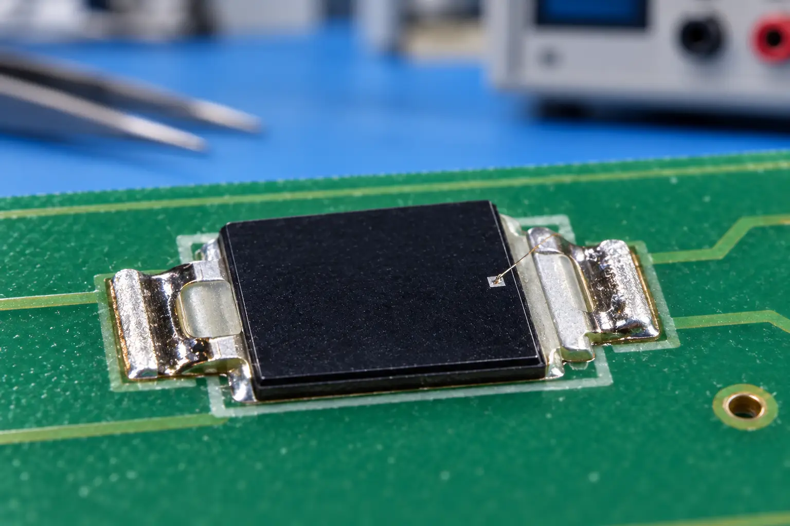
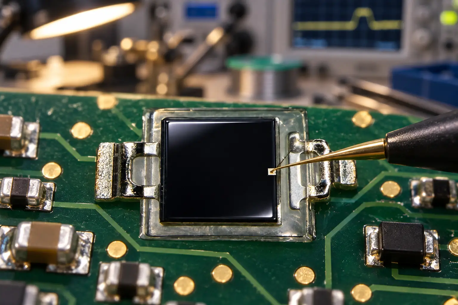
Si PIN photodiode PDCP08 Series PDCP08-511
The PDCP08-511 is a high-performance Black Epoxy PIN Photodiode designed for precision infrared applications. Encased in a special black epoxy resin, this sensor effectively acts as a daylight filter, blocking visible light interference while maximizing sensitivity at 940nm. With a large 2.9×2.9mm active area and low dark current, it ensures reliable signal detection for optical switches and remote control systems, even in noisy ambient light environments.
Inside an NIR Enhanced Silicon Photodiode: How the Sausage is Made
How do semiconductor fabs persuade stubborn near-infrared photons to stop inside the active collection zone? You cannot alter the fundamental bandgap of bulk silicon without turning to expensive III-V compound wafers like InGaAs or GaAs.
Instead, an NIR enhanced silicon photodiode relies on clever wafer engineering, deep depletion profiles, and photon management.
| Parameter / Feature | Standard Silicon PIN Diode | NIR Enhanced Silicon Photodiode |
|---|---|---|
| Wafer Material | Standard low-to-medium resistivity epi-wafer | High-resistivity float-zone silicon wafer |
| Depletion Layer (I-Region) | Thin (5 µm to 15 µm) | Extra-deep (40 µm to over 100 µm) |
| Surface Reflection | Standard visible AR coating (~30% NIR loss) | Multilayer dielectric AR coating tuned for 850-950nm (<1% loss) |
| Backside Treatment | Bare metal contact | Micro-textured optical trapping / dielectric back-reflector |
| Photon Fate @ 940nm | Punches through to substrate; lost via recombination | Absorbed in electric field or reflected back into depletion layer |
1. High-Resistivity, Deep Depletion Layers
Instead of standard epitaxial layers grown a few micrometers thick, an NIR enhanced silicon photodiode uses high-resistivity silicon float-zone wafers. High purity allows the intrinsic (I) region between the P and N layers to be stretched anywhere from 40 µm to over 100 µm thick. When reverse-biased, the depletion electric field extends completely through this thick slab without causing early dielectric breakdown. This gives deep-traveling 940 nm photons plenty of room to convert into carriers right inside the strong field.
2. Optical Trapping and Backside Reflectors
If a photon still manages to traverse a 60 µm depletion layer without hitting a silicon atom, high-grade NIR detectors do not let it escape out the back. Manufacturers introduce micro-textured surfaces or metallic backside reflection layers. Photons bounce off the rear surface at angled trajectories, doubling or tripling their optical path length through the depletion zone. This internal bounce is what turns a mediocre 40% QE device into an NIR enhanced silicon photodiode achieving >85% QE.
3. Tailored Antireflection (AR) Coatings
Bare polished silicon has a refractive index close to 3.5 in the near-infrared, reflecting roughly 30% of incident light right off the top window before it ever touches the active region. Standard photodiodes use silicon nitride or silicon dioxide coatings tuned for peak transmission around 550 nm or 632 nm. An NIR enhanced silicon photodiode uses quarter-wave dielectric stacks optimized specifically for the 850 nm to 950 nm band, dropping surface reflection losses under 1%.
Benchmarking the Hardware: Standard Si vs. NIR Enhanced vs. InGaAs
Engineers often ask: “Why not just jump straight to Indium Gallium Arsenide (InGaAs)?”
InGaAs is an incredible material. It offers stellar responsivity well past 1600 nm. But unless you are building a telecommunication transceiver running at 1550 nm or a high-end SWIR thermal camera, InGaAs will crush your bill of materials (BOM).
Here is how the technologies compare in real bench terms:
| Parameter | Standard Silicon PIN | NIR Enhanced Silicon Photodiode | InGaAs PIN Photodiode |
|---|---|---|---|
| Peak Spectral Range | 700 nm – 850 nm | 850 nm – 980 nm | 1100 nm – 1650 nm |
| Responsivity @ 850nm | 0.40 – 0.52 A/W | 0.58 – 0.64 A/W | ~0.20 – 0.35 A/W (Sub-optimal) |
| Responsivity @ 940nm | 0.20 – 0.38 A/W | 0.60 – 0.72 A/W | ~0.60 – 0.70 A/W |
| Dark Current (Typ. @ 25°C) | 0.1 – 1.0 nA | 0.2 – 2.0 nA | 1.0 – 10.0 nA |
| Junction Capacitance | Moderate | Low to Moderate (thick I-layer) | Low |
| Relative Unit Cost | $ (Baseline) | $$ (1.2x – 1.8x) | $$$$$ (10x – 30x) |
| Operating Temp Stability | Stable | Stable | Requires Temp Compensation |
As the data shows, using an NIR enhanced silicon photodiode gives you InGaAs-level responsivity at 940 nm while staying firmly rooted in low-cost, ultra-reliable silicon manufacturing.
Cutting LED Power and Extending Range: The Optical Link Budget
Let’s look at the basic math of an optical link. Whether you are building an automated guided vehicle (AGV) beam detector, a liquid level sensor, or an optical safety light curtain, your receiver photocurrent (I_photo) is governed by:
I_photo = P_optical * R
Where:
- P_optical is the optical power hitting the photodiode active area.
- R is the photodiode responsivity at your emitter wavelength.
Now consider an emitter pushing 940 nm light.
Suppose your optical setup drops 10 microwatts (-20 dBm) of power onto your detector surface:
- With a run-of-the-mill silicon sensor where R = 0.32 A/W:
I_photo = 10 µW * 0.32 A/W = 3.2 µA - Swap in a dedicated NIR enhanced silicon photodiode operating at R = 0.65 A/W:
I_photo = 10 µW * 0.65 A/W = 6.5 µA
That is a straight 103% increase in signal current.
What does this mean for your system architecture? You have two choices:
Option A: Halve Your Emitter Power Consumption
If your transimpedance amplifier (TIA) stage was already satisfied with 3.2 µA of photocurrent, you can cut your emitter LED drive current by half. For an industrial battery-powered IoT tracker, dropping LED pulse current from 60 mA to 30 mA directly extends field operating lifetime by months.
Option B: Extend Your Working Distance
In free-space optics, optical power density falls off according to the inverse-square law:
P_received is proportional to 1 / (Distance)^2
If your receiver responsivity jumps from 0.32 A/W to 0.65 A/W, your system can tolerate roughly double the path attenuation. Because path loss scales quadratically with distance:
Distance_new = Distance_old * square_root(R_new / R_old)
Distance_new = Distance_old * square_root(0.65 / 0.32) = Distance_old * 1.42
By doing nothing more than dropping an NIR enhanced silicon photodiode into your receiver circuit, you gain a 42% boost in sensing range without touching your emitter, optics, or power supplies.
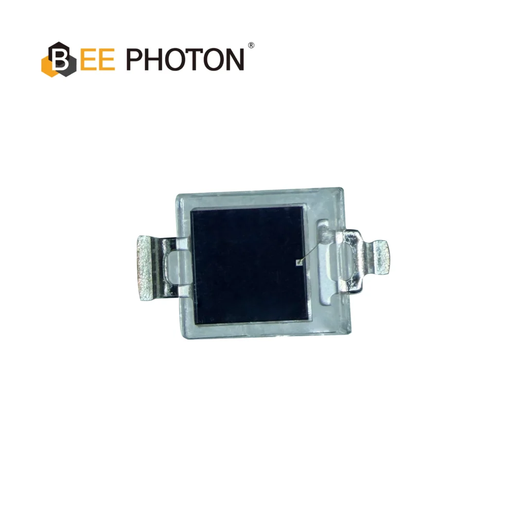
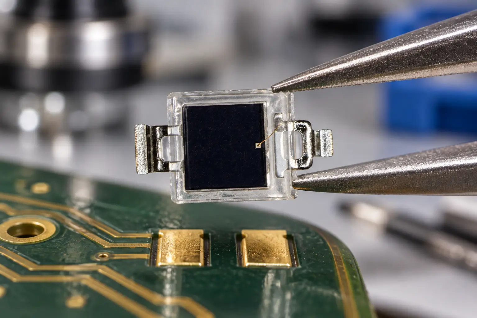
Si PIN photodiode PDCP08 Series PDCP08-501
High-Performance Detection: The PDCP08-501 is a high-speed Silicon PIN Photodiode with a transparent window.
Key Specs: Featuring a 2.9×2.9mm active area, this PIN photodiode offers low dark current and high responsivity, making it an ideal sensor for general optical switches and light detection systems.
Field Notes & Real-World Integration: Picking the Right Sensor
Every hardware design involves trade-offs. You cannot just pick a part based on responsivity alone; packaging, filtering, and junction area can make or break your noise floor.
Here is how experienced optical engineers match specific hardware to field challenges:
1. The Daylight Blinding Problem (Outdoor or Ambient Light)
If your sensor works in environments with fluorescent lighting or direct sunlight, ambient visible photons will flood your junction, driving your receiver into saturation.
In these setups, using a sensor with molded daylight-blocking encapsulation is essential. A great example of this execution is the PDCP08-511 black epoxy PIN photodiode. The black epoxy package acts as an integrated optical bandpass filter, blocking visible wavelengths below 750 nm while allowing near-infrared light around 850 nm and 940 nm to pass unhindered. This prevents ambient shot noise from eating your dynamic range.
2. Space-Constrained Layouts and High Packing Density
When building compact optical switches, miniature encoders, or handheld clinical monitors, bulky TO-can packages are out of the question. You need clean surface-mount technology (SMT) with consistent optical alignment.
For tight boards, components like the PDCP08-502 silicon PIN photodiode offer a low-profile 2.9×2.8mm SMD footprint. Its compact active area minimizes stray parasitics while maintaining high responsivity across the near-infrared band.
3. General-Purpose Industrial Sensing
For classic through-beam barriers, pulse meters, or reflective sorting gates, standard packages like the PDCP08-501 PIN photodiode provide an ideal middle ground between generous active area (making optical alignment forgiving on the factory floor) and low junction capacitance.
To browse full technical datasets, mechanical packages, and custom die configurations, explore the primary BeePhoton optical sensor portfolio for specialized commercial and industrial optoelectronics.
Practical Design Traps: Capacitance, Bandwidth, and Dark Current
Let’s address the potential snags. You do not get better near-infrared responsivity for free; physics always extracts a toll somewhere. When designing around an NIR enhanced silicon photodiode, watch these three traps:
1. Thick Depletion vs. Capacitance Trade-Off
The junction capacitance (Cj) of any PIN diode is determined by the parallel-plate equation:
Cj = (epsilon_r * epsilon_0 * Area) / Depletion_Width
Where:
- epsilon_r is the dielectric constant of silicon (~11.7)
- epsilon_0 is the permittivity of free space
- Area is the active photosensitive area
- Depletion_Width is the thickness of the depleted I-region
Because an NIR enhanced silicon photodiode intentionally uses a deeper depletion region (larger Depletion_Width) to absorb long-wavelength photons, its junction capacitance per unit area is actually lower than a shallow visible photodiode under full bias!
However, if you compensate for mechanical misalignment by choosing an oversized active area (say, 10 mm² instead of 1 mm²), your capacitance will shoot up into dozens of picofarads.
In a standard Transimpedance Amplifier (TIA), input capacitance combines with the op-amp’s internal input capacitance to form a pole in your feedback loop:
f_pole = 1 / (2 * pi * R_feedback * C_total)
This pole introduces phase lag, causing TIA ringing, peak gain instability, or outright oscillation.
TIA Stability Implementation Guide:
- Connect the photodiode cathode to your reverse bias supply (e.g., +3.3V or +5V) and anode to the inverting input of your operational amplifier.
- Tie the non-inverting input directly to analog ground.
- Place your main gain resistor (R_feedback) between the inverting input and the analog output.
- Always place a small ceramic compensation capacitor (C_feedback) in parallel with R_feedback to cancel the pole caused by the photodiode junction capacitance.
Calculate your feedback capacitor with this standard formula:
C_feedback = square_root( C_total / (2 * pi * R_feedback * Gain_Bandwidth_Product) )
2. Dark Current Drift Across Temperature
Because an NIR enhanced silicon photodiode utilizes thicker high-resistivity silicon, thermally generated carriers inside the depletion zone can be slightly higher than in specialized ultra-low-dark-current visible planar diodes.
Dark current roughly doubles every 8 to 10 degrees Celsius rise:
I_dark(T) = I_dark(25°C) * 2^((T – 25) / 10)
If you are measuring continuous wave (CW) optical power at DC, dark current drift will look just like signal drift.
- The Practical Fix: Modulate your emitter LED with a burst frequency (e.g., 10 kHz to 50 kHz) and pass your receiver signal through an analog high-pass filter or use synchronous detection (lock-in amplification). This strips away DC dark current drift, ambient daylight, and low-frequency 100/120 Hz indoor lighting ripple completely.
3. Apply Adequate Reverse Bias
Many engineers run photodiodes in photovoltaic mode (zero bias) to eliminate dark current entirely. While that works for slow, low-noise DC light meters, zero-bias operation leaves the depletion zone narrow.
Without reverse bias, your NIR enhanced silicon photodiode cannot fully clear its thick intrinsic layer, destroying both your near-infrared responsivity and your response time. Applying even 3.3V or 5V of reverse bias broadens the depletion layer fully, accelerating carrier drift velocity to saturation (~10^7 cm/s in silicon) and unlocking peak responsivity.
For high-accuracy laboratory references, the NIST Optical Detector Calibration group provides detailed methodologies on bias-dependent responsivity and quantum efficiency measurement techniques. You can also cross-reference detector testing protocols outlined by organizations like the SPIE Digital Library for solid-state NIR electro-optical performance.
Real-World Case Study: Overhauling a Warehouse Perimeter Curtain
To see how this works in practice, consider an industrial automation retrofit handled for an automated warehouse client.
The Problem
The client had a safety light curtain system spanning 12 meters across busy aisle openings. The original design used 940 nm LEDs pulsing at 20 kHz with standard silicon PIN receivers.
When dust built up on the lens covers or ambient warehouse dust scattered light, the system generated persistent false-alarm stops. The engineering team tried to resolve the issue by driving the 940 nm LEDs harder, pushing peak pulse current to 250 mA.
Within 6 months, emitter failure rates spiked. The LEDs ran hot, their wire bonds degraded, and internal epoxy turned brittle.
The Solution and Bench Results
Instead of burning through more LEDs, the team redesigned the receiver PCB to use an NIR enhanced silicon photodiode housed in daylight-filtering black epoxy (PDCP08-511).
Here are the side-by-side bench results before and after the retrofit:
| Operational Metric | Standard Si Receiver (Legacy) | NIR Enhanced Receiver (PDCP08-511) |
|---|---|---|
| Photodiode Responsivity | 0.28 A/W @ 940nm | 0.62 A/W @ 940nm (2.2x gain) |
| LED Drive Current | 250 mA (Peak Pulse) | 110 mA (Peak Pulse, -56% power) |
| Optical Head Temp Rise | +24°C above ambient | +6°C above ambient |
| Lens Dust Obscuration Tolerance | Fails at 15% light loss | Operates reliably up to 45% light loss |
The takeaway? Upgrading to an NIR enhanced silicon photodiode solved a thermal reliability failure while simultaneously making the optical link tough enough to handle dirty industrial environments.

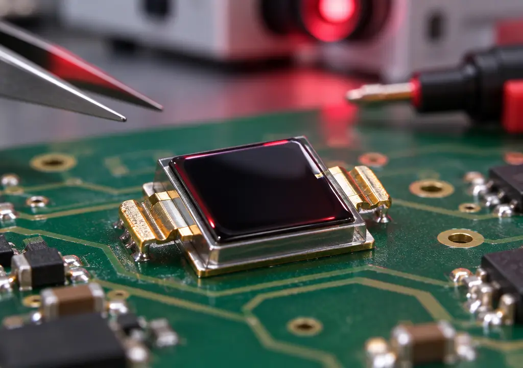
Si PIN photodiode PDCP08 Series PDCP08-502
The PDCP08-502 is a high-response 2.9×2.8mm Silicon PIN Photodiode designed for precision photoelectric applications. Featuring low junction capacitance, low dark current, and a wide spectral range (340-1100nm), it is the ideal component for optical switches and compact sensing modules requiring stable and fast signal output.
Frequently Asked Questions (FAQ)
Can an NIR enhanced silicon photodiode replace an InGaAs photodiode at 850nm and 940nm?
Yes, absolutely. In fact, an NIR enhanced silicon photodiode is generally better than an InGaAs detector at 850 nm and equal to it at 940 nm. InGaAs detectors typically have higher dark current, much higher unit costs, and sub-optimal responsivity below 900 nm due to surface recombination. Unless your application extends out past 1100 nm (such as 1310 nm or 1550 nm telecommunication bands), an NIR enhanced silicon photodiode is the superior engineering and commercial choice.
Why not just use an optical lens instead of an NIR enhanced photodetector?
Lenses can focus more light onto your detector, but they narrow your receiver’s Field of View (FOV). In many real-world systems—like smoke detectors, free-space optical switches, or touchless sensors—narrowing the field of view makes mechanical alignment difficult and makes the system hypersensitive to vibration. An NIR enhanced silicon photodiode provides higher electrical output without altering your system’s optical geometry or tightening mechanical assembly tolerances.
How does reverse bias voltage affect responsivity in an NIR enhanced silicon photodiode?
In standard visible photodiodes, reverse bias mainly improves bandwidth and reduces capacitance, with minor impact on responsivity. In an NIR enhanced silicon photodiode, however, reverse bias is essential to fully deplete the deep, high-resistivity intrinsic silicon layer. Without adequate reverse bias (typically between 3V and 15V depending on die thickness), deep-penetrating 940 nm photons will generate carriers in field-free diffusion zones, reducing effective responsivity and slowing pulse rise times.
Optimize Your Optical Link Budget with BeePhoton
Building high-performance optoelectronic systems is always an exercise in balancing compromises: power versus range, bandwidth versus active area, and BOM cost versus raw performance.
If your current near-infrared system is struggling with weak signal margins, excessive emitter heat, or limited range at 850 nm or 940 nm, stop overdriving your LEDs. The fastest, most robust way forward is upgrading your receiver to a specialized NIR enhanced silicon photodiode.
At BeePhoton, we engineer and manufacture precision silicon photodiodes tailored for demanding sensing, industrial automation, and optical telemetry applications. From daylight-filtering epoxy packages like the PDCP08-511 to compact SMD form factors like the PDCP08-502 and dependable through-hole workhorses like the PDCP08-501, our components give you the sensitivity your link budgets demand.
Ready to boost your receiver performance?
- Browse our technical portfolio: Visit the BeePhoton Product Catalog
- Consult directly with our engineering team: Reach out via our Contact Us Page
- Request test samples or volume pricing: Drop us an email at info@photo-detector.com
Send us your wavelength, target bandwidth, and package constraints, and let our application engineers help you select the ideal NIR enhanced silicon photodiode for your next production run.