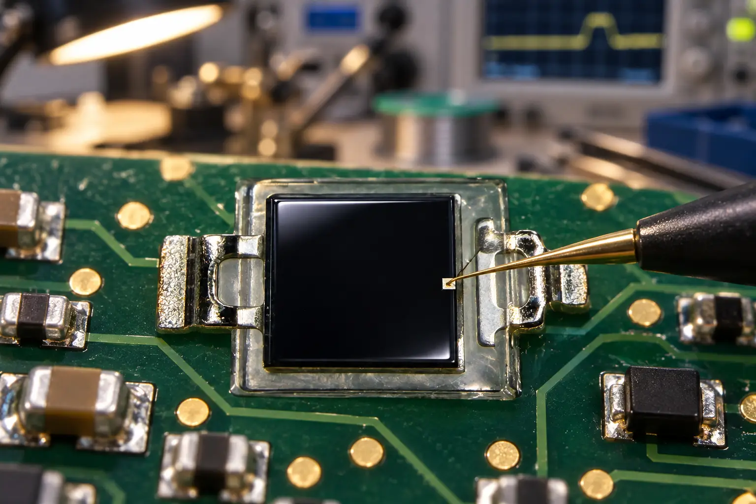
Designing optical front-ends that work seamlessly from near-ultraviolet right through the near-infrared is notoriously frustrating. If you have spent late nights in the lab debugging a high-speed industrial color mark sensor or an analytical benchtop instrument, you know the drill. You pick an optical detector that boasts terrific figures on paper at 850nm or 905nm, plug in a 465nm royal blue reference LED or a 340nm excitation lamp, and watch your signal-to-noise ratio dive straight off a cliff.
The physics behind that drop is simple, but solving it on a production bill of materials without blowing up unit costs is tricky. Standard silicon PN or PIN chips feature a thick passive p+ layer on their front surface. Ultraviolet and short visible photons dump all their energy within the first few tens of nanometers of silicon, right in that heavily doped dead zone where recombination wipes out carriers before the electric field can sweep them away.
That is precisely where an optimized visible-enhanced PIN photodiode changes the entire game. Instead of accepting miserable blue responsivity or stitching together two separate sensors with an expensive dichroic beam splitter, a properly engineered visible-enhanced PIN photodiode flattens the spectral response curve across the full 340nm to 1100nm span.
In this teardown, we will unpack how a visible-enhanced PIN photodiode alters junction mechanics, how to balance junction capacitance against responsivity in transimpedance loops, and how engineering teams integrate these detectors into high-speed packaging lines, water analytics, and clinical flow cytometry.
What Makes a Visible-Enhanced PIN Photodiode Different?
Most catalog silicon diodes are optimized for optical communications or infrared remotes, peaking somewhere between 850nm and 960nm. When you inspect their datasheets, responsivity at 400nm is often an embarrassing 0.08 A/W or worse.
A high-performance visible-enhanced PIN photodiode fundamentally modifies two core attributes of the silicon substrate: junction depth and the front anti-reflective coating stack.
A shallow junction is the difference between capturing an electron-hole pair generated by a 405nm photon and letting it turn into useless surface heat through recombination.
1. Ultra-Shallow Junction Engineering and the Recombination Dead Zone
High-energy visible light (such as 465nm blue) and UV-A (340nm–380nm) have an extremely short penetration depth in silicon. Per classic optical constant models documented by research repositories like IEEE Xplore, a 365nm photon is absorbed within less than 20 nanometers of the entry surface. Conventional silicon sensors feature an entry p-layer that extends several hundred nanometers deep.
In an industrial-grade visible-enhanced PIN photodiode, wafer fabrication relies on ultra-shallow boron diffusion or ultra-low-energy ion implantation. By keeping this dead layer under 30nm, the depletion region essentially borders the passivation layer. Photogenerated minority carriers encounter the electric field immediately, yielding a quantum efficiency above 70% in the visible band where ordinary chips give you 20% or less. When you deploy a visible-enhanced PIN photodiode, your short-wavelength signal is preserved right at the silicon interface.
2. Multi-Layer Anti-Reflective (AR) Optimization
Bare polished silicon behaves like a mirror for blue wavelengths, reflecting upwards of 45% of incident light at 400nm. While budget detectors use a single-layer silicon nitride coating tuned for 850nm, a high-responsivity visible-enhanced PIN photodiode uses alternating dielectric layers, typically silicon dioxide and titanium dioxide or silicon oxynitride.
This multi-layer coating flattens the reflection valley across the critical 380nm–750nm window. Rather than bouncing off the surface, incoming photons penetrate directly into the active silicon. This allows the visible-enhanced PIN photodiode to maintain steady broadband efficiency across the entire spectrum.

Si PIN photodiode PDCP08 Series PDCP08-511
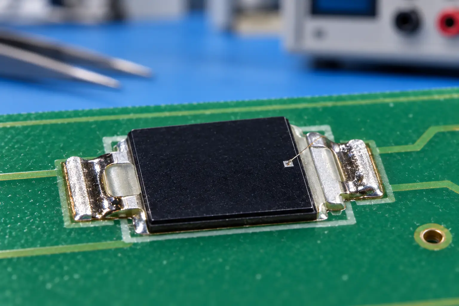
The PDCP08-511 is a high-performance Black Epoxy PIN Photodiode designed for precision infrared applications. Encased in a special black epoxy resin, this sensor effectively acts as a daylight filter, blocking visible light interference while maximizing sensitivity at 940nm. With a large 2.9×2.9mm active area and low dark current, it ensures reliable signal detection for optical switches and remote control systems, even in noisy ambient light environments.
Key Optical and Electrical Mechanics
When your hardware engineering team evaluates a visible-enhanced PIN photodiode, you cannot look at responsivity in a vacuum. You have to balance dark current, junction capacitance, and shunt resistance to ensure real-world circuit stability.
Responsivity Calculation
The baseline photocurrent output for any visible-enhanced PIN photodiode follows the fundamental photo-conversion relationship:
I_photo = P_in × R(λ)
Where R(λ) represents spectral responsivity in Amperes per Watt (A/W). You can express responsivity in terms of Quantum Efficiency (η) and wavelength (λ) using the standard identity:
R(λ) = (q · λ · η) / (h · c) ≈ (λ [in μm] / 1.24) · η
For instance, when your visible-enhanced PIN photodiode achieves an 80% quantum efficiency at 465nm:
R(465nm) ≈ (0.465 / 1.24) · 0.80 ≈ 0.30 A/W
On an un-enhanced silicon diode, quantum efficiency is lucky to hit 35% at that same wavelength, dragging your signal down to 0.13 A/W. That 2.3x raw signal boost from a visible-enhanced PIN photodiode translates directly into extra dynamic range before your first transimpedance amplifier gain stage even touches the signal.
Bandwidth vs. Capacitance Tradeoff
Speed is governed by two factors: transit time through the intrinsic region and the RC time constant formed by the diode junction capacitance (Cj) and feedback impedance. The cutoff frequency is given by:
f_3dB = 1 / (2 · π · R_load · C_j)
When selecting a visible-enhanced PIN photodiode, expanding the active area makes optical alignment much easier, but Cj climbs linearly with area. If you run a high-gain transimpedance amplifier for faint analytical signals, excessive junction capacitance from an oversized visible-enhanced PIN photodiode destabilizes your operational amplifier, causing peaking or full-blown oscillation.
Practical optical design tip: If your light pulse width is under 100ns, keep your active sensor area below 10 mm² unless you intend to run reverse bias over 10V to clamp down junction capacitance.
To keep your transimpedance loop stable without sacrificing speed, your feedback capacitor (Cf) should be calculated as:
C_f = [ C_in / (2 · π · R_f · GBW) ]^0.5
Where C_in combines your visible-enhanced PIN photodiode capacitance and op-amp common-mode input capacitance, and GBW is the amplifier gain-bandwidth product.
Thermal Drift and Shunt Resistance
Noise at zero bias (photovoltaic mode) is dominated by Johnson noise generated across the detector shunt resistance (Rsh). Noise Equivalent Power (NEP) is defined as:
NEP = [ (4 · k_B · T · B) / R_sh ]^0.5 / R(λ)
Where:
- k_B is Boltzmann’s constant (1.38 × 10^-23 J/K)
- T is absolute temperature in Kelvin
- B is noise bandwidth in Hertz
- R_sh is shunt resistance in Ohms
A well-passivated visible-enhanced PIN photodiode maintains high shunt resistance, often exceeding 500 MΩ at room temperature. This suppresses thermal noise so effectively that faint 340nm fluorescent returns can be captured from background noise without resorting to deep thermoelectric cooling. Working with an optimized visible-enhanced PIN photodiode gives your analog front end the quiet baseline it needs.
Comparing Visible-Enhanced PIN Photodiode Specs with Standard Sensors
To give you an honest baseline when writing your hardware component specification, here is how typical production detectors stack up against purpose-built optical silicon.
| Parameter | Standard Silicon PIN Diode | Visible-Enhanced PIN Photodiode | UV-Extended Photodiode |
|---|---|---|---|
| Spectral Range | 430nm – 1100nm | 340nm – 1100nm | 190nm – 400nm |
| Responsivity @ 365nm | < 0.05 A/W | 0.12 – 0.18 A/W | 0.20 – 0.24 A/W |
| Responsivity @ 465nm | 0.15 – 0.20 A/W | 0.28 – 0.35 A/W | < 0.05 A/W (Blind) |
| Responsivity @ 628nm | 0.38 – 0.42 A/W | 0.42 – 0.48 A/W | Near Zero |
| Responsivity @ 905nm | 0.60 – 0.65 A/W | 0.58 – 0.63 A/W | Ineffective |
| Dark Current (Vr=10V) | 0.5 – 2.0 nA | 0.2 – 1.0 nA | 1.0 – 5.0 nA |
| Capacitance Density | ~40 pF/mm² | ~25 – 35 pF/mm² | High (>50 pF/mm²) |
| Typical Packaging | Molded clear epoxy | TO-can, SMD ceramic, filtered resin | Quartz window / Ceramic |
Looking at these figures, you can see why the visible-enhanced PIN photodiode is considered an industry workhorse. It sustains solid responsivity across red and near-infrared channels while preserving high sensitivity across blue and near-UV channels, avoiding the sharp infrared cutoff inherent to specialized UV-only chips. For broadband instrumentation, a single visible-enhanced PIN photodiode handles the workload of two separate narrow-band sensors.
The Signal Chain Architecture
Understanding where your detector sits inside the overall optoelectronic instrument helps optimize board routing and optical coupling.
Receiver Signal Chain Flow:
- Target Light Input (340nm–1100nm broadband, laser lines, or strobed LED channels).
- Visible-Enhanced PIN Photodiode: Collects incident photons with shallow p+ junction and wideband anti-reflective coating to output linear photocurrent (I_photo).
- Transimpedance Amplifier (TIA Stage): Converts microamp/nanoamp photocurrent into low-impedance analog voltage using a low-noise operational amplifier.
- Active Filtering & Digitization: Multi-pole active bandpass filter feeds into a 16-bit or 24-bit high-speed ADC for digital signal processing.
When you install a visible-enhanced PIN photodiode as the primary front-end transducer in this signal chain, the initial gain stage does not need to be cranked to extreme values. This directly preserves signal bandwidth and reduces operational amplifier phase margin issues.
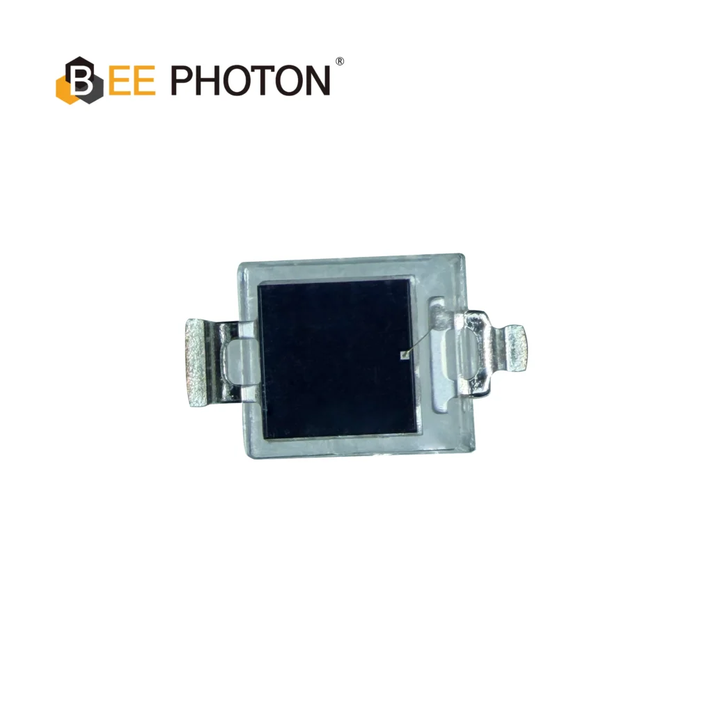
Si PIN photodiode PDCP08 Series PDCP08-501
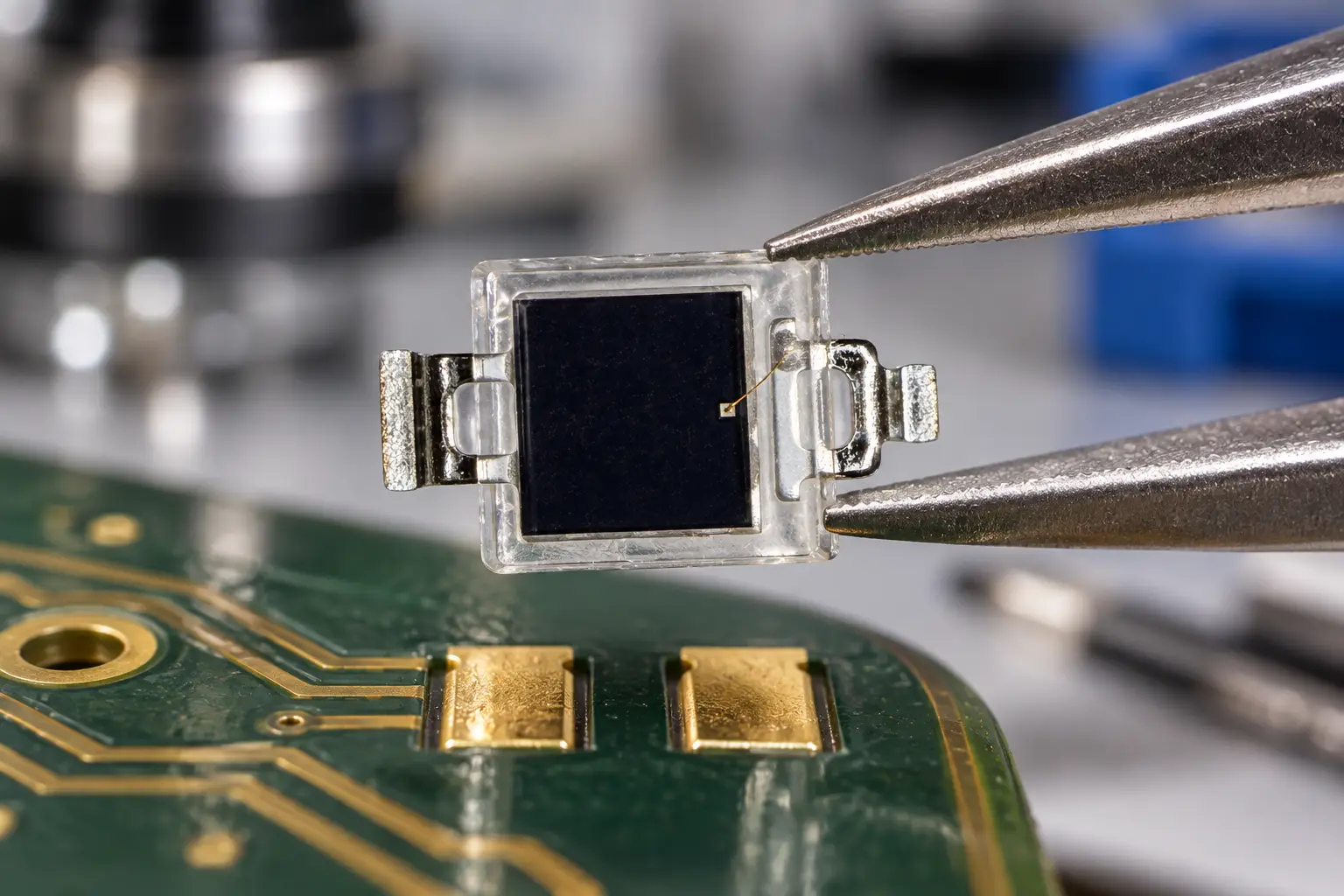
High-Performance Detection: The PDCP08-501 is a high-speed Silicon PIN Photodiode with a transparent window.
Key Specs: Featuring a 2.9×2.9mm active area, this PIN photodiode offers low dark current and high responsivity, making it an ideal sensor for general optical switches and light detection systems.
Practical Applications: Where the Rubber Meets the Road
Let’s look past the raw specs at where engineers are actively deploying a visible-enhanced PIN photodiode on factory automation floors and inside clinical diagnostic hardware.
1. High-Speed Industrial Color Mark Sensors (465nm / 628nm Detection)
Packaging equipment running blister packs, poly-films, and tube printing relies on registration mark sensors switching at frequencies up to 50 kHz. The optical head frequently combines a high-speed tricolor emitter (465nm blue, 525nm green, 628nm red) that strobes sequentially against print targets moving at several meters per second.
If you place a standard infrared-leaning diode into that receiver, the signal output from the 628nm red strobe will dwarf the 465nm blue reflection by more than a factor of three, even when looking at a neutral gray registration target. Your analog stage requires complex variable gain compensation or dual potentiometers to avoid clipping the ADC input.
By contrast, using a balanced PDCP08-502 visible-enhanced PIN photodiode levels the playing field completely. Its 2.9×2.8mm active footprint provides an ideal collection angle without requiring complex secondary focusing optics, while delivering balanced photocurrent across blue and red strobes. Packaging engineers can verify fundamental PIN detector mechanics through comprehensive technical overviews on RP Photonics. Using a calibrated visible-enhanced PIN photodiode ensures reliable contrast discrimination on glossy substrates with minimal software normalization.
2. Analytical Chemistry & Flow Cytometers
Flow cytometers interrogate biological cells labeled with fluorophores as they stream through a microfluidic flow cell. Excitation typically occurs via 405nm violet or 488nm blue lasers, with emissions radiating anywhere from 520nm (FITC channel) all the way out to 785nm (PerCP-Cy5.5 or Alexa Fluor dyes).
Hardware engineers frequently face a dilemma: should they specify photomultiplier tubes, avalanche photodetectors, or a visible-enhanced PIN photodiode?
While photomultiplier tubes offer massive internal gain, their physical size, kilovolt operating voltages, and drift over time create major reliability headaches in field-deployed clinical equipment. For forward scatter, side scatter, and high-emission fluorescent channels, an ultra-low-noise visible-enhanced PIN photodiode backed by a precision JFET-input operational amplifier provides an extremely reliable, solid-state channel.
For setups where out-of-band visible noise must be rejected while collecting specific emission bands, opting for specialized packaging like the PDCP08-511 black epoxy PIN photodiode helps block stray room illumination. When wide-spectrum collection across all visible channels is mandatory, the versatile PDCP08-501 broadband photodiode serves as an ideal baseline sensor. In each of these analytical setups, the broad responsivity of a visible-enhanced PIN photodiode simplifies multi-channel optical routing.
3. Spectrophotometry and Water Quality Turbidity Meters
Modern multi-parameter water analysis instruments measure total organic carbon, chlorine residual, and turbidity within a single optical chamber. Doing this requires measuring 340nm UV absorbance (for nitrates and organic compounds), 550nm absorbance (for standard colorimetric chemical reagents), and 860nm scattering per the ISO 7027 water quality testing protocol outlined by ISO International Standards.
A single visible-enhanced PIN photodiode covers all three measurement points without breaking a sweat. That eliminates the electromechanical filter wheels or multi-sensor configurations that introduce mechanical failure modes and calibration drift across seasonal temperature shifts. Implementing a visible-enhanced PIN photodiode gives environmental instrumentation teams a durable, solid-state sensing path.
Layout and Circuit Traps That Will Ruin Your Signal
Selecting high-grade silicon is only half the battle. Screwing up the printed circuit board layout around your visible-enhanced PIN photodiode can easily waste the premium optical responsivity you paid for.
Here are three real-world hardware oversights observed during optoelectronic board bring-ups:
Pitfall 1: Stray Guard Traces and Parasitic Leakage
When running a visible-enhanced PIN photodiode in photovoltaic mode (zero bias) for ultra-low noise, dark current drops into the single-digit picoamp range. A single solder flux smudge or slight ambient humidity can create board surface leakage currents of tens of nanoamps, completely swamping your microamp-level photo-response.
Layout Rule: Always route an unbroken copper guard ring completely encircling the anode and cathode pads of your visible-enhanced PIN photodiode. Drive that guard ring to the same potential as the inverting input of your transimpedance amplifier. This clamps surface leakage to zero, keeping your noise floor down at the physical limit.
Pitfall 2: Neglecting the Reverse-Bias Noise Penalty
Reverse-biasing your visible-enhanced PIN photodiode slashes junction capacitance and widens your bandwidth, which is essential for megahertz optical communications. However, every volt of reverse bias injects shot noise caused by dark leakage current:
I_shot = (2 · q · I_dark · B)^0.5
If your application does not require megahertz bandwidth (such as an analytical turbidity meter sampling at 1 kHz), avoid running high reverse bias. Run your visible-enhanced PIN photodiode at zero bias into a precision rail-to-rail CMOS or JFET amplifier. You trade away a few nanoseconds of transient response, but you gain an ultra-quiet, drift-free baseline signal.
Pitfall 3: Window Material Cutoffs
It sounds basic, but many optical teams overlook window transmission. An engineer selects a high-grade visible-enhanced PIN photodiode rated down to 340nm, then seals the external enclosure with a standard polycarbonate or soda-lime glass protective window.
Standard glass exhibits a sharp transmission cutoff starting right around 380nm, completely blinding the sensor to light at 340nm. If your instrument requires the full spectrum of the visible-enhanced PIN photodiode, always specify optical-grade fused silica, quartz, or borosilicate (such as Schott N-BK7) cover optics. Make sure your visible-enhanced PIN photodiode packaging uses an optical-grade silicone or transparent epoxy resin.
Procurement Checklist: Selecting the Right Visible-Enhanced PIN Photodiode
Before signing off on your bill of materials or issuing a production purchase order, verify these engineering items with your optical sensor supplier:
- Responsivity Floor: Does the visible-enhanced PIN photodiode maintain at least 0.25 A/W at your lowest critical operating wavelength (e.g., 405nm or 465nm)?
- Active Area Geometry: Have you balanced your optical alignment tolerances against junction capacitance? A larger visible-enhanced PIN photodiode die eases mechanical alignment, but higher capacitance slows down your amplifier.
- Temperature Stability: Check the temperature coefficient across your operating range. While silicon responsivity drifts at 900nm (roughly +0.2%/°C), the 400nm–600nm visible spectrum exhibits exceptional stability (<0.02%/°C) when using a visible-enhanced PIN photodiode.
- Packaging Reliability: Will an SMD package survive your reflow profile, or does your vibration profile demand a TO-can? Check package mechanical drawings on the BeePhoton Product Catalog to match your optical enclosure.
- Traceable Sensor Standards: For medical diagnostics or regulated safety devices, ensure your photodiode batch testing aligns with radiometric calibration standards traceable to NIST or equivalent metrology authorities. A reliable visible-enhanced PIN photodiode vendor will supply full calibration curves on request.

Si PIN photodiode PDCP08 Series PDCP08-502
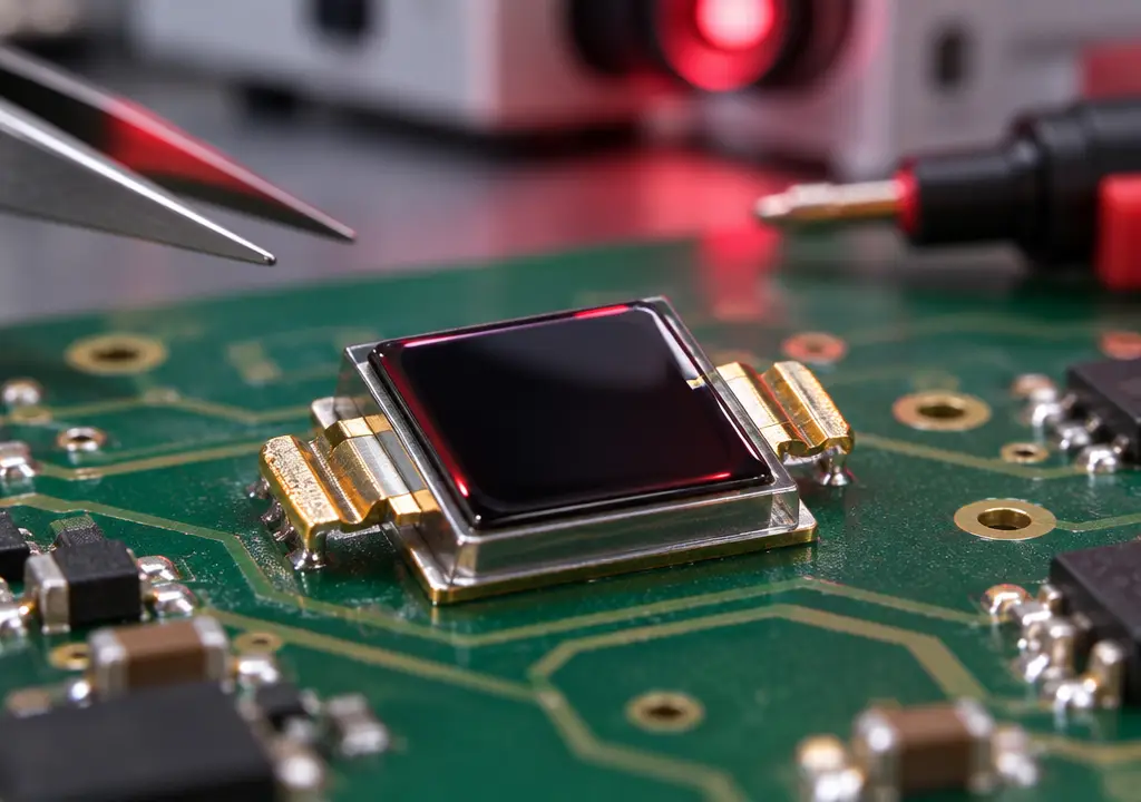
The PDCP08-502 is a high-response 2.9×2.8mm Silicon PIN Photodiode designed for precision photoelectric applications. Featuring low junction capacitance, low dark current, and a wide spectral range (340-1100nm), it is the ideal component for optical switches and compact sensing modules requiring stable and fast signal output.
Frequently Asked Questions
Why not use a standard phototransistor instead of a visible-enhanced PIN photodiode?
Phototransistors have internal gain, which looks attractive at first glance. However, they suffer from terrible non-linearity, high temperature drift, and sluggish rise and fall times that often exceed 15 microseconds. A visible-enhanced PIN photodiode provides linear output current across 6 to 8 decades of light intensity, making it far superior for calibrated color measurement, pulse detection, and precision spectroscopy.
Does reverse bias boost the responsivity of a visible-enhanced PIN photodiode?
No. Unlike avalanche photodiodes, applying reverse bias to a visible-enhanced PIN photodiode does not increase its internal responsivity (A/W). Internal quantum efficiency stays constant. Reverse bias simply widens the internal depletion layer, reducing junction capacitance to speed up transient switching, with a minor penalty in dark current.
Can a visible-enhanced PIN photodiode detect UV-C wavelengths below 280nm?
Generally, no. A standard visible-enhanced PIN photodiode is optimized down to approximately 320nm or 340nm. Deep UV-C photons (200nm–280nm) absorb right at the outer passivation boundary, causing rapid solarization of epoxy packages. For UV-C disinfection or flame detection, wide-bandgap Silicon Carbide (SiC) or Gallium Nitride (GaN) detectors are much better suited than a silicon visible-enhanced PIN photodiode.
What distinguishes the BeePhoton PDCP08-502 from the PDCP08-501?
While both are built on precision silicon technology, the PDCP08-502 visible-enhanced PIN photodiode features a 2.9×2.8mm active area designed specifically to balance low junction capacitance with easy beam alignment in compact color mark sensors. The PDCP08-501 offers an alternate active area geometry optimized for general broadband sensing and higher optical collection angles.
Accelerate Your Optical Sensor Pipeline
If you are struggling with poor blue-channel signal-to-noise ratios, inconsistent color discrimination on packaging equipment, or noisy fluorescence channels in clinical instruments, legacy detector architectures are wasting your engineering cycles.
Integrating a purpose-built visible-enhanced PIN photodiode into your analog front end fixes short-wavelength degradation right at the silicon surface.
At BeePhoton, we design and manufacture high-reliability optical detectors built for demanding industrial automation and analytical applications. Whether you are ramping up a multi-channel color sensor assembly or developing next-generation laboratory diagnostics:
- Review Technical Specifications: Compare spectral curves, capacitance specs, and package outlines across our complete BeePhoton Photodiode Lineup.
- Request Engineering Samples & Quotes: Submit your transimpedance bandwidth targets, mechanical constraints, and target volumes through the BeePhoton Contact Page.
- Consult Our Optical Engineers: Send your schematic questions, target wavelength list, and custom packaging requirements directly to our technical team at info@photo-detector.com.
Stop trying to compensate for inadequate front-end sensor responsivity in firmware. Upgrade your optical hardware with a high-responsivity visible-enhanced PIN photodiode and capture the complete spectrum from 340nm to 1100nm with total confidence.