If you have ever had a field maintenance engineer call you at two in the morning because an automated bottling line suddenly ground to a halt inside an unconditioned warehouse in the middle of summer, you already know the culprit. On paper, the bench prototype back at your air-conditioned development lab functioned like a charm. The comparator snapped cleanly at 500 millivolts, the microcontroller recorded every passing edge, and your unit cost looked fantastic. Then that same equipment went into mass production, got mounted six inches away from a variable-frequency conveyor motor inside an unventilated IP67 enclosure, and phantom switching events began ruining factory efficiency.
At the heart of this recurring nightmare sits a silent silicon parameter that far too many hardware teams neglect during parts selection: dark current thermal drift. Specifying an industrial photoelectric sensor diode is rarely about finding maximum spectral responsivity under pristine room conditions. It is about preserving your optical detection margins when ambient operational temperatures swing across an unforgiving -40°C to +100°C window.
Let us dig into why ambient heat plays havoc with optical detection thresholds, break down the physics behind thermal drift optical sensor degradation, and explore how picking an optimized industrial photoelectric sensor diode keeps your automation hardware running reliably when real-world conditions turn harsh.
Why Factory Floors Wreck Standard Optical Sensing Margins
Factory environments are notoriously rough on sensitive optoelectronics. Unlike telecom transceivers housed in climate-regulated server rooms, an industrial photoelectric sensor diode frequently operates bolted right next to injection molding heaters, high-torque servo drives, curing ovens, or outdoor sub-zero logistics gantries. Standard consumer-grade photodiodes simply give up under these relentless thermal swings.
When local temperatures rise, thermal vibrations through the silicon crystal lattice ramp up sharply. If your industrial photoelectric sensor diode lacks an optimized junction profile, that thermal agitation begins tearing electron-hole pairs loose across the depletion zone without a single photon striking the detector surface. This phantom output current is your dark current, and its thermal behavior is notoriously aggressive.
“A sensor designer who ignores thermal drift is not building an optical switch; they are building an unpredictable solid-state thermometer.”
For any hardware developer building a wide temperature range sensor, the real trouble is not merely that leakage current increases. It is that dark current creates a constantly moving baseline voltage. If your analog decision circuit assumes a zero-watt optical floor, every 10°C jump in enclosure temperature steals away your signal-to-noise ratio (SNR), pulling the entire industrial photoelectric sensor diode setup into false positive lockouts or dropped pulses.
The Dark Current Temperature Coefficient (TCID) Explained
To understand how an industrial photoelectric sensor diode behaves when environmental conditions shift, we need to inspect its dark current temperature coefficient, typically labeled in datasheets as TCID.
In Silicon P-N and PIN structures, reverse leakage current is caused by thermal generation-recombination inside the space-charge depletion region, accompanied by minority carrier diffusion from adjacent neutral silicon. As outlined in fundamental optoelectronic references like the Wikipedia overview of photodiode physics, reverse dark current climbs exponentially alongside rising temperature.
The underlying solid-state equation governing reverse saturation leakage current across temperature is expressed as:
I_dark(T) = I_0 * (T / T_0)^(3/2) * exp(-E_g / (2 * k_B * T))
In this expression:
- I_dark(T) represents dark current at absolute junction temperature T (in Kelvin).
- I_0 represents a manufacturing process constant.
- E_g represents the silicon bandgap energy (roughly 1.12 eV at room temperature).
- k_B represents the universal Boltzmann constant (8.617 x 10^-5 eV/K).
Out on the factory workbench, calculating exponential bandgap dynamics in real time is impractical. Analog designers instead rely on the empirical parameter known as the photodiode temperature coefficient for dark current (TCID):
I_dark(T) = I_dark(25°C) * (TCID)^(T – 25)
For a conventional silicon junction, TCID photodetector values hover around 1.13 per degree Celsius (1.13/°C). That multiplier seems harmless at first glance, until you calculate the compound growth across an industrial thermal swing.
Because 1.13 multiplied across a 6-degree interval yields approximately 2.08, your reverse dark current doubles roughly every 6°C to 8°C.
Consider a generic silicon photodiode with an initial baseline dark current of 2 nA at 25°C. When ambient heating pushes the sensor housing up to 85°C—a realistic 60°C temperature climb—the math yields startling numbers:
I_dark(85°C) = 2 nA * (1.13)^60 ≈ 2 nA * 1,480 ≈ 2.96 µA
What began as a negligible 2 nanoamps has exploded into nearly 3 microamps of pure thermal leakage. If your analog transimpedance amplifier uses a 1-megohm feedback resistor, that thermal surge injects a massive 2.96-volt DC offset. On a standard 3.3V or 5V single-supply rail, your amplifier output slams hard against the positive power rail. Your industrial photoelectric sensor diode is now completely blinded.

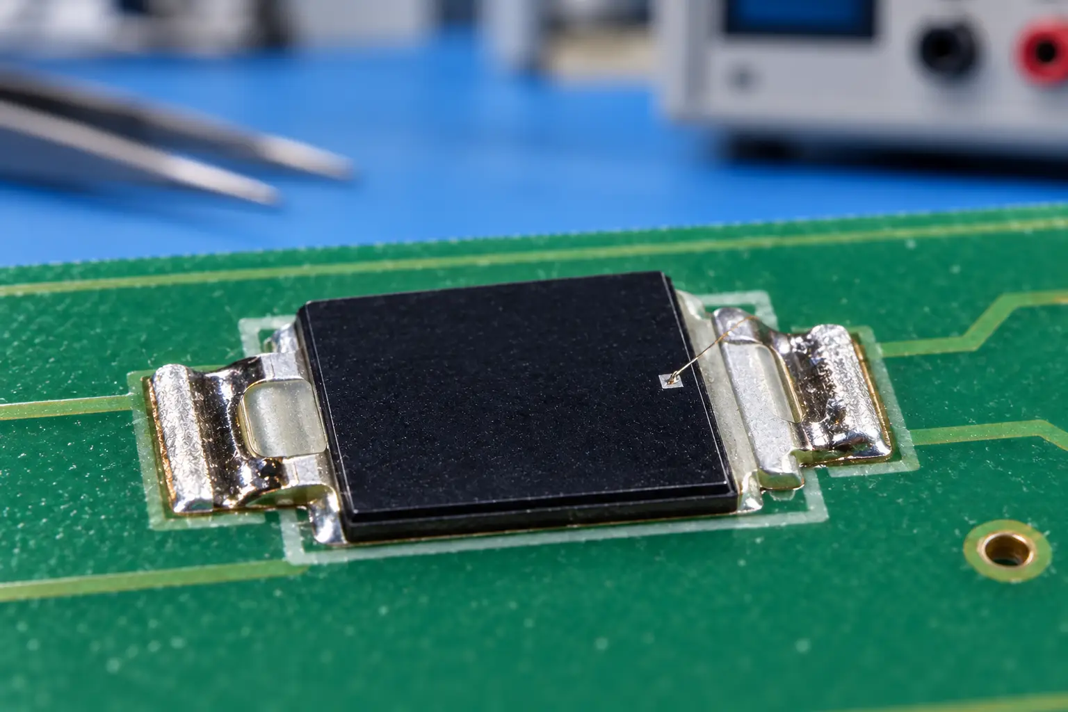
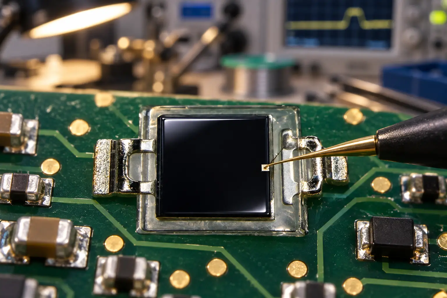
Si PIN photodiode PDCP08 Series PDCP08-511
The PDCP08-511 is a high-performance Black Epoxy PIN Photodiode designed for precision infrared applications. Encased in a special black epoxy resin, this sensor effectively acts as a daylight filter, blocking visible light interference while maximizing sensitivity at 940nm. With a large 2.9×2.9mm active area and low dark current, it ensures reliable signal detection for optical switches and remote control systems, even in noisy ambient light environments.
Shunt Resistance (Rsh) Collapse at Elevated Temperatures
Dark current leakage is only one half of the equation. The second failure point that blindsides system designers is the severe thermal collapse of shunt resistance (Rsh).
Shunt resistance measures the slope of the photodiode current-voltage characteristic curve around zero bias. Pristine silicon PIN dies measured at 25°C often exhibit an Rsh climbing into hundreds of megaohms or several gigaohms. However, as operating temperatures climb toward 70°C, 85°C, or 100°C, internal carrier generation causes shunt resistance to plunge, as characterized across global testing frameworks like the IEC 60747-5-5 optoelectronic device standards.
Why does falling shunt resistance ruin an otherwise sound optical layout? In an unbiased photovoltaic transimpedance amplifier (TIA), the operational amplifier’s intrinsic input voltage noise (e_n) gets multiplied by the front-end circuit noise gain:
Noise Gain = 1 + (R_feedback / R_shunt)
When R_shunt drops from 500 MΩ down to 500 kΩ under hot factory conditions, your circuit noise gain increases by hundreds of times. This magnifies voltage offsets and high-frequency operational amplifier noise right at the analog output pin, totally unrelated to any actual light entering the aperture. When sourcing a high-reliability industrial photoelectric sensor diode, verifying that the silicon junction retains high shunt resistance across high temperatures is just as critical as baseline dark current.
Benchmarking Diode Performance Across Industrial Temperature Spans
Not every photodiode die configuration handles severe thermal swings equally. Here is an honest engineering comparison showing how common optical detector types behave across an industrial temperature envelope (-40°C to +100°C).
| Operational Parameter | Commercial Plastic PIN Diode | BeePhoton Industrial Silicon PIN | Avalanche Photodiode (APD) |
|---|---|---|---|
| Room Temp Dark Current (25°C) | 2 nA to 10 nA | 0.5 nA to 2 nA | 1 nA to 15 nA |
| Dark Current at 85°C | 1.5 µA to 8 µA | 0.1 µA to 0.6 µA | Catastrophic (> 25 µA, runaway risk) |
| Effective TCID | ~ 1.15 / °C | ~ 1.11 to 1.13 / °C | Extreme (Requires bias compensation) |
| Shunt Resistance at 85°C | Collapses < 1 MΩ | Sustained > 15 MΩ | Non-applicable (Operates reverse biased) |
| Package Durability | Clear standard epoxy | Daylight Black Epoxy / TO-Can | Hermetic TO with TEC integration |
| Bill of Materials Cost | Very Low ($) | Moderate ($$) | Very High ($$$$) |
| Primary Industrial Use | Office automation, clean rooms | Packaging, machine safety, sorting | Precision distance LiDAR, lab optics |
While Avalanche Photodiodes offer spectacular optical multiplication factors, their internal avalanche gain fluctuates wildly with temperature, demanding costly high-voltage feedback loops or active Peltier coolers. For standard industrial machinery, an optimized silicon PIN industrial photoelectric sensor diode delivers the best balance of price, repeatability, and rugged reliability—provided the thermal leakage curve has been properly controlled.
Packaging Matters: Conquering Ambient Factory Interference
Managing thermal drift optical sensor performance is not strictly a silicon die problem. The package molding enclosing your semiconductor die plays an equally critical role in industrial uptime.
Visible-Light Filtering Resin
Most industrial sorting gates, safety curtains, and retro-reflective arrays utilize infrared light emitters operating around 850 nm or 940 nm. If you drop an industrial photoelectric sensor diode built with transparent clear resin onto an active shop floor, ambient illumination from overhead LED high-bays, welding arcs, and inspection lamps floods the silicon die. That uncontrolled illumination burns up amplifier headroom long before your target reflector breaks the beam.
By compounding optical dye filters directly into the packaging epoxy, the package completely blocks visible ambient light between 400 nm and 700 nm while allowing target infrared wavelengths to pass virtually unhindered. A field-proven implementation is the BeePhoton Si PIN photodiode PDCP08-511, which incorporates a visible-light cutoff black epoxy package designed to eliminate ambient factory floor glare and suppress stray optical shot noise.
Surface Mount vs. Through-Hole Mechanical Dissipation
Package construction also governs junction heat dissipation. Miniature surface mount devices (SMDs) streamline automated pick-and-place assembly, but they sit flat against PCB copper layers that carry heat from nearby power MOSFETs, motor drivers, and switching regulators.
When selecting a compact SMD industrial photoelectric sensor diode for tight spaces, reviewing the thermal dissipation layout is vital. For space-restricted sensor heads, the BeePhoton 2.9×2.8mm Silicon PIN Photodiode PDCP08-502 provides a low-profile footprint designed to retain mechanical alignment and stable thermal performance inside miniature IP-rated enclosures.
When your mechanical housing requires extra physical distance between the detector junction and a scorching PCB, standard radial leaded packages like the BeePhoton Silicon PIN Photodiode PDCP08-501 allow technicians to bend leads, direct the optical angle, and elevate the sensitive silicon away from hot circuit board zones.
How Thermal Drift Destroys Detection Thresholds
When an uncalibrated industrial photoelectric sensor diode suffers from excessive dark current thermal drift, it does not just shift your DC baseline. It also injects significant shot noise straight into your front-end analog signal chain.
Total shot noise current (i_sn) produced by an industrial photoelectric sensor diode under reverse bias or active light exposure is governed by the classic shot noise equation:
i_sn = sqrt(2 * q * (I_photo + I_dark) * B)
Where:
- q represents the elementary electronic charge (1.602 x 10^-19 Coulombs).
- I_photo represents the actual photocurrent produced by target illumination.
- I_dark represents thermal leakage dark current.
- B represents the operational analog bandwidth of your receiver stage.
When I_dark multiplies by several orders of magnitude on a hot summer afternoon, your shot noise current floor climbs rapidly.
Signal Threshold Breakdown Across Temperature Spans
- Standard Operation at 25°C:
Dark Baseline Voltage = 0.05 V
Target Light Pulse Peak = 3.20 V
Fixed Comparator Switching Threshold = 1.60 V
Result: Robust 1.55 V noise margin. Switching is crisp, fast, and free of jitter.- Thermal Drift Failure at 85°C:
Dark Baseline Voltage = 1.95 V (shifted +1.90 V due to thermal dark current)
Noise Ripple Window = 1.65 V to 2.25 V
Fixed Comparator Switching Threshold = 1.60 V
Result: Baseline voltage and thermal noise ride completely above the switching threshold. The sensor locks into an uninterrupted false-trigger state with zero optical beam interruption.
This comparison illustrates why standard fixed-voltage trigger designs crumble when ambient temperatures shift. Without thermal baseline management or an inherently low-drift industrial photoelectric sensor diode, automated systems will drop packets, stall machinery, and produce endless troubleshooting tickets.
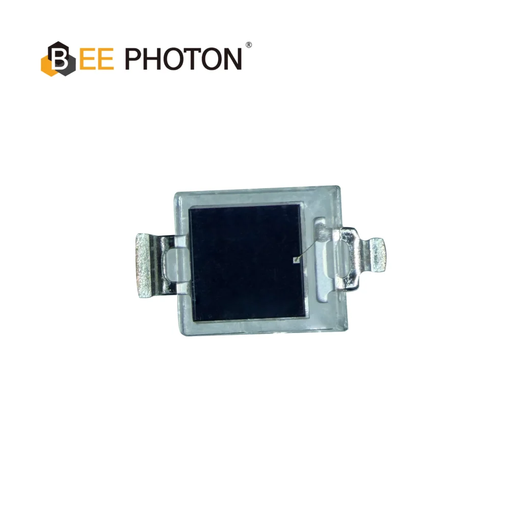
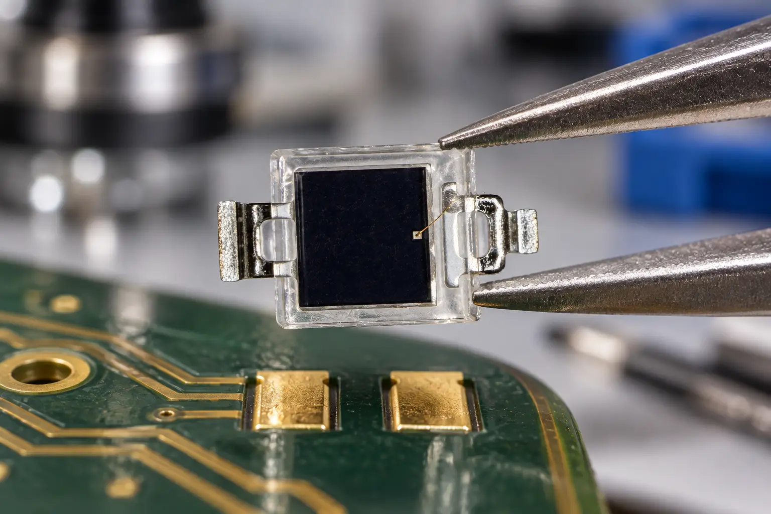
Si PIN photodiode PDCP08 Series PDCP08-501
High-Performance Detection: The PDCP08-501 is a high-speed Silicon PIN Photodiode with a transparent window.
Key Specs: Featuring a 2.9×2.9mm active area, this PIN photodiode offers low dark current and high responsivity, making it an ideal sensor for general optical switches and light detection systems.
Circuit Design Tactics to Tame Thermal Drift
While sourcing an industrial photoelectric sensor diode with an engineered low TCID photodetector profile forms your strongest hardware safeguard, pairing it with smart analog front-end (AFE) topologies creates a truly bulletproof system.
1. Zero-Bias Photovoltaic Mode
If your optical switching frequency allows moderate rise times (below 1 MHz), run your industrial photoelectric sensor diode in zero-bias photovoltaic mode. By maintaining both anode and cathode pins at identical DC potentials, reverse dark current drops close to zero:
I_dark(V_bias = 0) ≈ 0
In photovoltaic operation, the dominant thermal threat shifts from exponential dark current runaway to shunt resistance degradation and op-amp input offset voltage drift (V_os). Be sure to choose precision operational amplifiers with ultra-low thermal offset drift (sub-microvolt per °C). Technical design guidance from organizations like the IEEE Xplore Digital Library highlights that keeping junction bias below 10 mV is the single most effective way to eliminate exponential dark current drift in precision optical equipment.
2. AC-Coupled Modulated Illumination
Never run an unmodulated continuous-wave (CW) optical beam in an industrial environment if you can avoid it. Instead, drive your LED or laser emitter with a distinct carrier frequency (such as 15 kHz to 50 kHz) and route your TIA output through an analog high-pass filter:
f_cutoff = 1 / (2 * pi * R * C)
Any slow, wandering DC offset generated by dark current thermal drift or ambient temperature rise is blocked as near-DC noise by the series capacitor. The downstream comparator or ADC only processes the clean, carrier-modulated optical pulses.
3. Matched Blind Diode Cancellation
In high-precision measurement applications where DC optical accuracy cannot be sacrificed—such as optical turbidity monitoring, smoke detection, or fluid concentration analysis—place a secondary industrial photoelectric sensor diode immediately beside your active sensor diode. Mask this secondary diode with an opaque light shield so no photons can enter.
Wire both photodiodes in an opposing parallel or differential input configuration. Because both silicon dies sit at the identical enclosure temperature, their dark currents track each other closely. The matching dark current cancels out at the differential amplifier inputs, leaving only the genuine optical signal intact.
Field Case: Retrofitting AGV Sensors for Extreme Cold Storage
To appreciate how these thermal factors play out on real equipment, consider an automated materials handling manufacturer operating autonomous guided vehicles (AGVs) moving between an ambient indoor warehouse (+25°C) and a deep-freeze food storage warehouse (-35°C).
Their navigation safety units utilized off-the-shelf optical proximity sensors to detect structural racking uprights. While traveling through the warm packaging room, the optical sensors worked flawlessly. However, within minutes of an AGV entering the freezer bay, the sensors began missing close-proximity structural racks. Even worse, when returning to the warm environment, rapid thermal expansion caused sporadic false emergency stops, halting the vehicle in main transit corridors.
Diagnostic teardowns revealed three distinct failure mechanisms:
- The standard optical detector experienced a noticeable responsivity drop at -35°C because the silicon bandgap widened, shifting the peak absorption wavelength away from the 940 nm emitter. (Detailed spectral temperature shift charts can be referenced through the NIST Physical Measurement Laboratory).
- The front-end comparator threshold had been calibrated for room-temperature baseline current, causing cold-state offsets to plunge below the detection window.
- Rapid thermal cycling caused cheap clear epoxy lenses to develop microscopic internal stress cracks around the copper leadframe.
The engineering team resolved the problem by retrofitting the assembly with an industrial photoelectric sensor diode from BeePhoton. The new detector featured a high-purity silicon die with flat temperature stability, encapsulated in black daylight-blocking resin rated for severe thermal shock. The circuit was converted to zero-bias photovoltaic operation, and the emitter was adjusted to 880 nm to better match the cold-shifted silicon absorption band.
The outcome? The AGV fleet racked up more than 18,000 operational hours across the -35°C to +25°C temperature transition without a single thermal false stop, cutting unscheduled line maintenance calls to zero.
Engineering Checklist for Selecting an Optical Diode
Before you sign off on a bill of materials based solely on cheap catalog pricing or peak responsivity metrics measured strictly at 25°C, put your candidate industrial photoelectric sensor diode through this engineering checklist:
- Demand Dark Current Maximums at Temperature Extremes: Insist on reviewing verified dark current specifications at +85°C and +100°C, rather than settling for standard room-temperature averages.
- Inspect the Shunt Resistance (Rsh) Minimums: Confirm that shunt resistance remains high enough at top operating temperatures to prevent severe transimpedance noise gain escalation.
- Select Optical Filtration Suited to Factory Light: Choose an industrial photoelectric sensor diode built with daylight-filtering black epoxy whenever your design operates in high-ambient-light industrial facilities.
- Review Thermal Shock Compliance: Check whether the package construction meets industrial testing profiles like AEC-Q101 or equivalent thermal cycling regimes (-40°C to +105°C) to prevent die bond failures over years of thermal cycling.
Selecting an optimized industrial photoelectric sensor diode early in your development cycle prevents expensive production redesigns, catastrophic field recalls, and frustrated end customers.

Si PIN photodiode PDCP08 Series PDCP08-502
The PDCP08-502 is a high-response 2.9×2.8mm Silicon PIN Photodiode designed for precision photoelectric applications. Featuring low junction capacitance, low dark current, and a wide spectral range (340-1100nm), it is the ideal component for optical switches and compact sensing modules requiring stable and fast signal output.
Frequently Asked Questions
What causes dark current to increase so rapidly in an industrial photoelectric sensor diode?
Dark current in an industrial photoelectric sensor diode is driven primarily by thermal generation-recombination within the silicon depletion zone. Because thermal electron-hole generation scales exponentially with temperature—dictated by the silicon bandgap energy and Boltzmann physics—dark current doubles roughly every 6°C to 8°C. Across an industrial gradient from 25°C to 85°C, leakage current can increase by more than 1,000 times.
How does thermal drift impact digital switching sensors compared to analog measurement sensors?
In digital switching sensors (such as through-beam gates or object counters), dark current thermal drift lifts the baseline voltage toward the comparator switching threshold, causing false triggers and output jitter. In analog measurement instruments (like optical power meters or turbidity sensors), thermal drift causes zero-offset drift and damages dynamic range, introducing measurement errors unless dynamic temperature compensation circuits are present.
Can firmware calibration completely solve photodiode temperature drift?
Firmware calibration can track slow baseline drift if a dedicated temperature sensor is placed right beside the photodiode. However, firmware cannot recover dynamic range if an operational amplifier has already drifted into power supply rail saturation. Furthermore, digital math cannot eliminate the physical shot noise introduced by high dark current. The most reliable solution pairs an intrinsically low-drift industrial photoelectric sensor diode with intelligent baseline tracking firmware.
What is the primary difference between photovoltaic and photoconductive operation regarding temperature drift?
Photovoltaic mode operates the photodiode with zero applied reverse bias (0V). This stops reverse dark current generation, minimizing thermal baseline shift, though junction capacitance is higher. Photoconductive mode applies a reverse bias voltage across the diode to achieve high switching speed and wide bandwidth, but it exposes the circuit to severe exponential dark current runaway whenever ambient temperatures climb.
Build Tougher Optical Systems with BeePhoton
Developing optical sensing equipment that performs consistently under demanding factory conditions requires optoelectronic components you can trust. A generic photodiode may look fine on an engineer’s workbench, but high-temperature conveyor belts, outdoor logistics yards, and automotive engine bays do not forgive thermal instability.
At BeePhoton, we engineer and manufacture precision optical detection components built specifically for severe operational conditions. Whether your next project demands a specialized industrial photoelectric sensor diode encapsulated in ambient-blocking black epoxy, miniature surface-mount devices for tight sensor heads, or customized silicon geometries with elevated shunt resistance, our engineering team is ready to assist.
Stop losing development time to phantom switching and thermal noise drift. Contact our optical engineering specialists today or email us directly at info@photo-detector.com to discuss your performance requirements, request evaluation samples, and receive a volume quotation for your next production run. Let us help you ensure rock-solid optical detection across every degree of your operating range.