Wenn Sie als Hardware-Ingenieur Ihr nächstes PCB-Layout entwerfen, haben Sie wahrscheinlich den Moment erreicht, in dem Sie innehalten und sich fragen: Soll ich eine Durchsteck-Fotodiode oder eine SMD-Fotodiode wählen? Das ist kein winziges Detail. Die Entscheidung zwischen SMD- und Durchgangsloch-Fotodioden hat Auswirkungen auf alle Bereiche, vom Platzbedarf auf der Leiterplatte und der Bestückungsgeschwindigkeit bis hin zur langfristigen Zuverlässigkeit und sogar darauf, wie sich das Ding verhält, wenn Licht auf es trifft. Ich habe Jahre bei BeePhoton damit verbracht, den Leuten zu helfen, genau dieses Problem zu lösen, und glauben Sie mir, es gibt keine pauschale Antwort. Aber lassen Sie uns das gemeinsam durchgehen, so wie wir es bei einem Kaffee tun würden: keine Floskeln, nur echte Gespräche darüber, was für Ihr Design wirklich wichtig ist.
Schnelle Aufschlüsselung: Was genau sind Durchsteck- und SMD-Fotodioden?
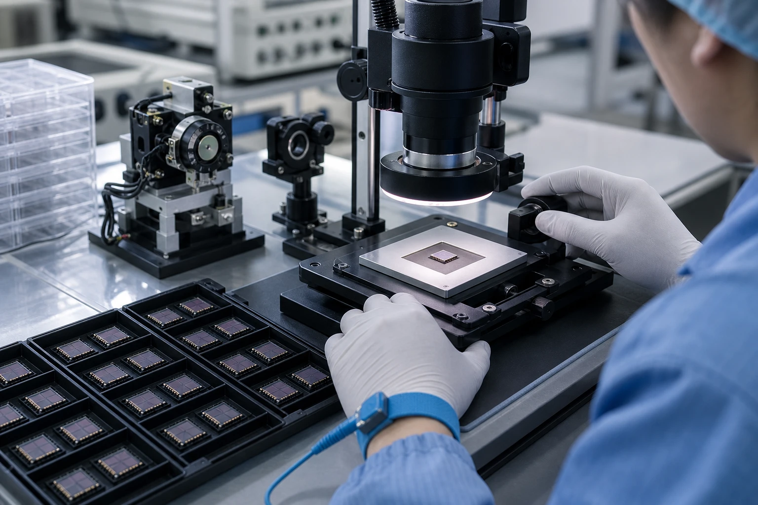
Durchgangsloch-Fotodioden haben diese klassischen Drahtanschlüsse, die gerade durch gebohrte Löcher in der Leiterplatte ragen. Man lötet sie auf der anderen Seite an, und sie sitzen schön fest. Der Unterschied zwischen SMD- und Durchgangsloch-Fotodioden beginnt hier - die oberflächenmontierten Versionen überspringen die Löcher komplett. Ihre winzigen Kontakte sitzen flach auf Kupferpads und werden in einem schnellen Durchgang durch den Ofen geklebt und reflowed.
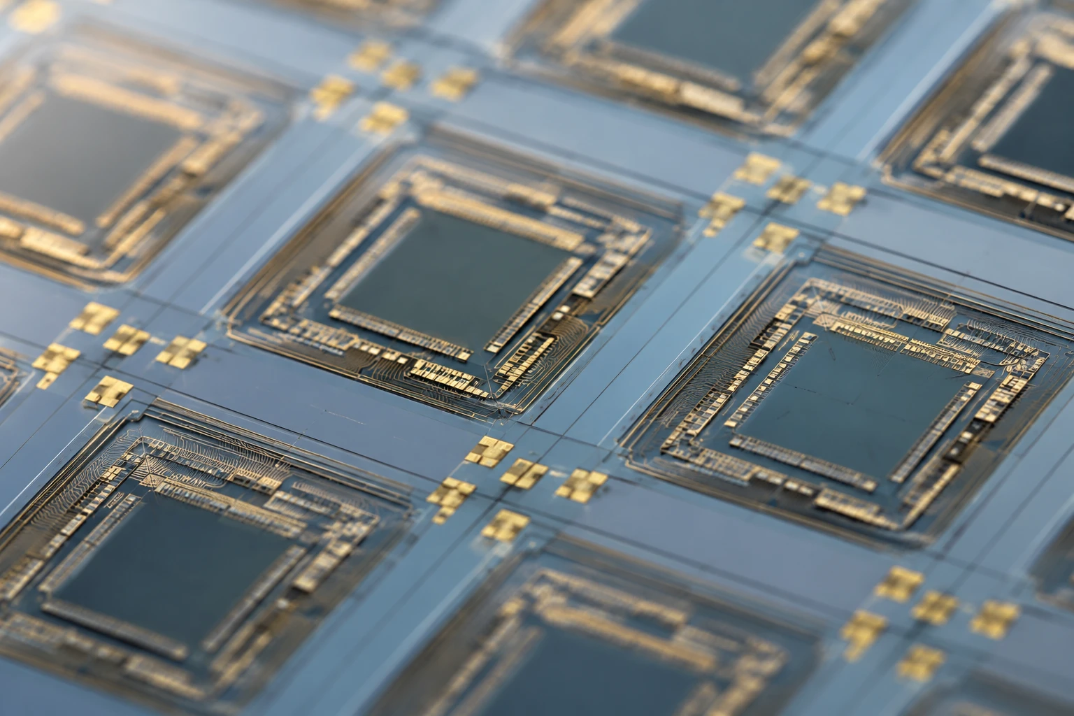
Bei beiden Typen handelt es sich heutzutage in der Regel um Si-PIN-Photodioden, da sie eine schnelle Reaktion, eine gute Empfindlichkeit im sichtbaren und nahen IR-Bereich sowie ein geringes Rauschen für die meisten Sensoraufgaben bieten. Aber das Gehäuse ändert das Spiel. Ein durchkontaktiertes Bauteil kann in einer TO-18-Metalldose oder einem Kunststoffgehäuse mit längeren Beinen untergebracht sein. SMD-Versionen passen in winzige 0805-Gehäuse oder kundenspezifische Flachgehäuse, die viel Platz sparen.
Warum das Gehäuse bei SMD- und Through-Hole-Photodioden eine größere Rolle spielt, als Sie denken
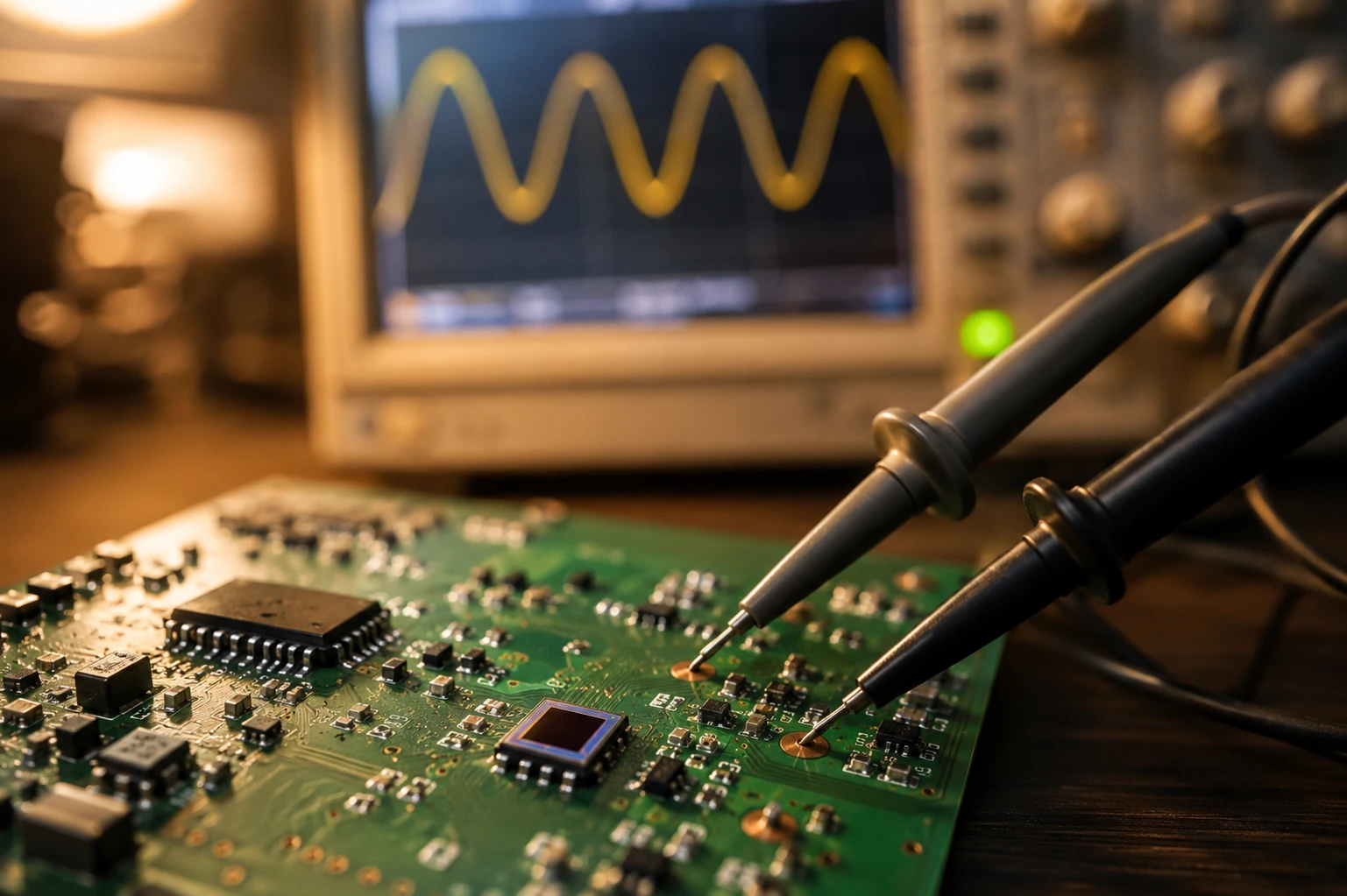
In den meisten Datenblättern wird diese Sache nicht erwähnt. Das Gehäuse ist nicht nur eine Hülle - es wirkt sich auf die parasitäre Induktivität, die Kapazität, den Wärmefluss und sogar darauf aus, wie viel Licht den aktiven Bereich tatsächlich erreicht. Bei der optischen Hochgeschwindigkeitsabtastung verringern kürzere Leitungen auf SMD-Fotodioden die Induktivität, was sauberere Signale bei MHz-Frequenzen bedeutet. Lange Leitungen bei durchkontaktierten Bauteilen? Sie wirken wie kleine Antennen und können Rauschen verursachen, insbesondere oberhalb von einigen hundert kHz.
Auf der anderen Seite bieten diese Durchgangsbohrungen einen felsenfesten mechanischen Halt. Wenn Ihre Leiterplatte in einer vibrierenden Maschine oder in einem Auto unter der Motorhaube arbeiten soll, ist dieser zusätzliche Halt wichtig. SMD-Verbindungen verlassen sich hauptsächlich auf die Stärke der Lötfäden, die für die meisten Verbraucherprodukte ausreichen, aber bei starken Erschütterungen brechen können.
Si-PIN-Photodioden-Array Vier-Quadranten-PD PDCA04-102
Auf der Suche nach einem leistungsstarken B2B Si-PIN-Photodioden-Array für die Präzisionserfassung? Die PDCA04-102 ist ein hochwertiger Vier-Quadranten-Detektor, der für industrielle OEM-Anwendungen entwickelt wurde. Mit einem robusten 16,5×14,5 mm Gehäuse mit vier großen 5×5 mm großen lichtempfindlichen Elementen bietet dieses Array eine außergewöhnliche Konsistenz und Empfindlichkeit für Positionserfassungs- und Laserausrichtungssysteme. Arbeiten Sie mit Bee Photon zusammen, wenn es um zuverlässige Massenfertigung und kundenspezifische Lösungen geht.
Kopf-an-Kopf-Vergleich: SMD vs. Through-Hole Photodiode - Spezifikationen, die wirklich zählen
Lassen Sie mich das in einer einfachen Tabelle darstellen, damit Sie nicht zehn Datenblätter wälzen müssen.
| Aspekt | Durchgangsloch-Photodiode | SMD-Fotodiode | Gewinner für die meisten PCB-Designs? |
|---|---|---|---|
| Größe und Platz auf der Tafel | Größere Grundfläche, benötigt gebohrte Löcher | 50-80% kleiner, für beide Seiten der Tafel | SMD |
| Montagegeschwindigkeit | Langsamer, oft Hand- oder Wellenlöten | Vollautomatisches Pick-and-Place, 5-10x schneller | SMD |
| Mechanische Festigkeit | Hervorragend - die Kabel halten sie fest | Gut, aber abhängig von den Lötstellen | Durchgangsbohrung |
| Leistung bei hohen Frequenzen | Höhere parasitäre Induktivität von Leitungen | Geringere Induktivität, besser für schnelle Signale | SMD |
| Wärmeableitung | Anständig, aber die Leitungen können als Hitzepfade fungieren | Näher am Kupfer der Leiterplatte, oft bessere thermische | Leichte Kante zum SMD |
| Prototyping & Reparatur | Super einfach - nehmen Sie einfach einen Lötkolben | Knifflig ohne Heißluft oder Rework-Station | Durchgangsbohrung |
| Kosten bei hohem Volumen | Höher aufgrund von Bohrungen und langsamerer Montage | Untere - Skalen schön | SMD |
| Vibrations-/Stoßbeständigkeit | Oberste Ebene | Solide, braucht aber einen guten Lötprozess | Durchgangsbohrung |
| Typischer Dunkelstrom | Ähnlicher nA-Bereich (abhängig vom Chip, nicht vom Gehäuse) | Ähnlich, aber kleinere Pakete können kühler laufen | Krawatte |
Zahlen wie die 5-10fach schnellere Bestückung stammen aus echten Industrie-Benchmarks für SMT-Leitungen im Vergleich zu Durchstecklöchern. Und ja, eine IEEE-Studie über die Zuverlässigkeit von Bauteilen zeigte, dass SMD-Aufbauten in kontrollierten Umgebungen eine um 37% niedrigere Fehlerquote aufweisen - vor allem, weil das automatisierte Löten viel konsistenter ist.
Wie SMD vs. Through-Hole Photodiode die realen Leistungszahlen beeinflusst
Reden wir über Formeln, ohne uns zu verzetteln. Der Fotostrom, den Ihre Schaltung tatsächlich sieht, ist ziemlich einfach: Fotostrom (Iph) ist gleich Empfindlichkeit (S in A/W) mal einfallende optische Leistung (P in Watt). Die meisten Si-PIN-Photodioden bewegen sich im sichtbaren Bereich zwischen 0,4 und 0,6 A/W. Der Gehäusetyp ändert nicht viel an der Chip-Physik, aber er beeinflusst, wie viel Licht tatsächlich auf den Chip fällt und wie schnell man das Signal auslesen kann.
Der Dunkelstrom (Id) - die schleichende Leckage, wenn es stockdunkel ist - liegt bei beiden normalerweise im niedrigen nA-Bereich. Aber in SMD-Gehäusen kann die geringere thermische Masse die Sperrschicht in dichten Layouts kühler halten, wodurch Id in der Praxis niedriger bleibt. Die Reaktionsgeschwindigkeit hängt von der Anschlusskapazität (Cj) plus Lastwiderstand ab. Ein niedrigeres Cj in vielen SMD-Designs (dank der engeren Geometrie) bedeutet, dass man höhere Grenzfrequenzen erreicht, bevor das Signal abklingt.
Bei einem Projekt, das wir für einen Industriesensor durchgeführt haben, konnte durch den Wechsel von einer Durchsteck- zu einer SMD-Fotodiode die Leiterplattengröße um fast 40% verringert und die Abtastrate um 25% erhöht werden, da die parasitären Anteile reduziert wurden. Der Kunde bemerkte keinen Rückgang der Empfindlichkeit - er profitierte sogar ein wenig von der besseren Lichteinkopplung in dem flacheren Gehäuse.
Wenn Durchgangsloch-Photodioden immer noch absolut sinnvoll sind
Schreiben Sie Durchstecklöcher nicht ab, nur weil SMD im Trend liegt. Wenn Sie Prototypen oder Kleinserien bauen, geht nichts über das einfache Handlöten und den schnellen Austausch von Teilen. In rauen Umgebungen - z. B. im Motorraum von Kraftfahrzeugen, in Industrieanlagen im Freien oder in Bereichen mit ständigen Vibrationen - ist die mechanische Verriegelung von Durchstecklöchern immer von Vorteil. Wir haben schon erlebt, dass SMD-Bauteile unter Laborbedingungen gut überlebt haben, um dann nach sechs Monaten unter realen LKW-Vibrationen zu reißen.
Wenn Ihr Design eine höhere Belastbarkeit oder größere aktive Flächen zum Sammeln von schwachem Licht benötigt, können Sie mit Durchsteckgehäusen oft größere Chips herstellen, ohne exotische (und teure) kundenspezifische SMD-Footprints verwenden zu müssen.
Si-PIN-Photodiode mit erhöhter NIR-Empfindlichkeit (430-1100nm) PDCP08-201
Die PDCP08-201 ist eine leistungsstarke SMD-Si-PIN-Fotodiode entwickelt für optische Präzisionskommunikation und medizinische Sensorik.[1] Mit einer großen aktiven Fläche von 2,9×2,9 mm, einer verbesserten NIR-Empfindlichkeit (0,70 A/W) und einem extrem niedrigen Dunkelstrom (20 pA) bietet dieser SMD-Si-PIN-Fotodiode gewährleistet eine hervorragende Signalerkennung und Zuverlässigkeit in einem kompakten oberflächenmontierten Gehäuse.
Wenn SMD-Fotodioden bei der Auswahl moderner PCB-Bauteile den Kürzeren ziehen
High-Density-Verbraucher- oder IoT-Produkte? Ganz klar SMD. Ihre Platine wird kleiner, leichter und billiger in der Herstellung, und Sie können die Komponenten auf beiden Seiten verdoppeln. Automatisierte Fertigungsstraßen lieben sie - weniger Arbeitsaufwand, weniger Fehler, schnellere Markteinführung. Außerdem ermöglicht das flache SMD-Profil die Montage direkt neben Linsen oder Fasern ohne zusätzliche Abstandshalter für die optische Ausrichtung in engen Räumen.
Bei BeePhoton sehen wir viele Projekte für medizinische Wearables und tragbare Analysatoren, die vollständig in SMD ausgeführt werden, weil jeder Millimeter zählt. Ein Kunde reduzierte seine Stücklistenkosten um 18% und die Leiterplattendicke um 30%, indem er seine Si-PIN-Photodioden auf oberflächenmontierte Versionen umstellte.
Real-World Anwendungsszenarien, die wir gesehen haben
Ein Beispiel ist der kompakte Umweltmonitor, den ein Kunde entwickelt hat. Das ursprüngliche Layout mit Durchgangslöchern funktionierte, aber die Platine war zu groß für das Gehäuse. Wir wechselten zu unseren SMD-Si-PIN-Fotodioden, verlegten sie ein wenig um und siehe da: dieselbe Empfindlichkeit, nur halb so groß, und nach einer kurzen Anpassung des Lötprofils bestanden sie den Vibrationstest mit Bravour.
Ein anderer Fall: ein industrieller Barcode-Scanner, der in einer staubigen Fabrik stand. Man blieb bei Durchgangsloch-Fotodioden, weil die Techniker vor Ort die Sensoren bei der Wartung schnell austauschen mussten. Die Reparaturzeit sank von 45 Minuten auf unter 10 Minuten. Unterschiedliche Anforderungen, unterschiedliche Gewinner beim Kräftemessen zwischen SMD- und Durchgangsloch-Fotodioden.
Kurztipps für die Auswahl des Richtigen für Ihr nächstes Layout
Beginnen Sie mit Ihren Beschränkungen. Wenig Platz und hohes Volumen? SMD. Prototyping oder robuste Umgebung? Durchgangsbohrung. Gemischt? Viele Platinen sind gemischt aufgebaut - SMD für das Fotodioden-Array und Durchgangsbohrung für die Anschlüsse.
Informieren Sie sich frühzeitig über die Möglichkeiten Ihres Montagebetriebs. Einige Geschäfte berechnen zusätzliche Gebühren für Durchgangsbohrungen. Schauen Sie sich auch das aktuelle Datenblatt für die von Ihnen gewählte Si-PIN-Fotodiode an - nicht alle Gehäuse sind gleich, selbst innerhalb der gleichen Serie.
Und vergessen Sie nicht die Wärmeentwicklung. Dichte SMD-Layouts können insgesamt heißer laufen, so planen Sie Ihre Kupfer gießt und vielleicht einen winzigen Kühlkörper Pad unter der Fotodiode hinzufügen, wenn youre Pushing hohe Sperrvorspannung.
Zusammenfassung der Entscheidungen zwischen SMD- und Durchgangsloch-Photodioden
Was ist also besser? Das kommt darauf an - aber jetzt haben Sie die echten Details statt allgemeiner Ratschläge. Die meisten modernen Designs sind in Bezug auf Kosten, Größe und Geschwindigkeit auf SMD ausgelegt, aber die Nischen für hohe Zuverlässigkeit und Prototypen werden nach wie vor von der Durchkontaktierung eingenommen. Am klügsten ist es, wenn Sie beide in Ihrer tatsächlichen Anwendungsschaltung testen. Das ist der Punkt, an dem der Gummi auf die Straße trifft.
Wenn Sie mit diesem Recht jetzt für Ihre PCB ringen, haben wir Sie. BeePhoton baut hochwertige Si-PIN-Fotodioden sowohl in Durchsteck- als auch in SMD-Gehäusen, und wir können Ihnen helfen, die perfekte Lösung zu finden. Besuchen Sie unser Kontaktseite oder senden Sie eine E-Mail an info@photo-detector.com. Nennen Sie uns Ihre Layout-Vorgaben und Lichtverhältnisse - wir geben Ihnen noch am selben Tag eine schnelle Empfehlung und einen Preisvorschlag. Wir wollen Ihnen nichts aufschwatzen, sondern nur ehrlich helfen, damit Ihr Entwurf in der Praxis auch wirklich funktioniert.

Si-PIN-Photodiode mit erhöhter NIR-Empfindlichkeit (350-1100nm) PDCC100-501
Erzielen Sie einheitliche Ergebnisse mit unserer High Consistency Si PIN Diode für medizinische Geräte. Diese COB-Photodiode bietet eine zuverlässige NIR-Empfindlichkeit für die Gesundheitsüberwachung. Vertrauen Sie unserer High Consistency Si PIN Diode.
FAQ
Was ist der größte praktische Unterschied beim Vergleich zwischen SMD- und Durchgangsloch-Fotodioden auf einer echten Leiterplatte?
Größe und Montage. SMD-Versionen schrumpfen Ihre Leiterplatte drastisch und laufen problemlos durch automatisierte Fertigungsstraßen, während die Durchsteckmontage zwar eine kugelsichere mechanische Festigkeit bietet, aber mehr Platz und Zeit in Anspruch nimmt.
Ist eine durchkontaktierte Fotodiode bei vibrationsintensiven Anwendungen immer zuverlässiger als eine SMD-Diode?
Meiner Erfahrung nach so ziemlich ja. Die Anschlüsse halten viel besser als Lötpads allein. Wir haben gesehen, dass SMD-Teile nach sorgfältigem Design halten, aber die Durchkontaktierung hat einfach diesen zusätzlichen Spielraum.
Wie entscheide ich mich bei einem neuen Hardware-Projekt zwischen SMD- und Durchgangsloch-Fotodioden?
Listen Sie Ihre Prioritäten auf: Platz auf der Leiterplatte, Produktionsvolumen, Reparaturbedarf und Umwelt. Holen Sie sich dann Muster von Lieferanten wie uns bei BeePhoton und testen Sie sie in Ihrer tatsächlichen Schaltung. Die Daten schlagen die Theorie jedes Mal.
Kann ich SMD- und Durchgangsloch-Fotodioden auf derselben Platine kombinieren?
Auf jeden Fall - viele Konstruktionen tun genau das. Verwenden Sie SMD für dichte Sensoranordnungen und Durchgangsbohrungen, wenn Sie robuste Steckverbinder oder einen einfachen Austausch im Feld benötigen. Planen Sie Ihren Lötprozess einfach sorgfältig.