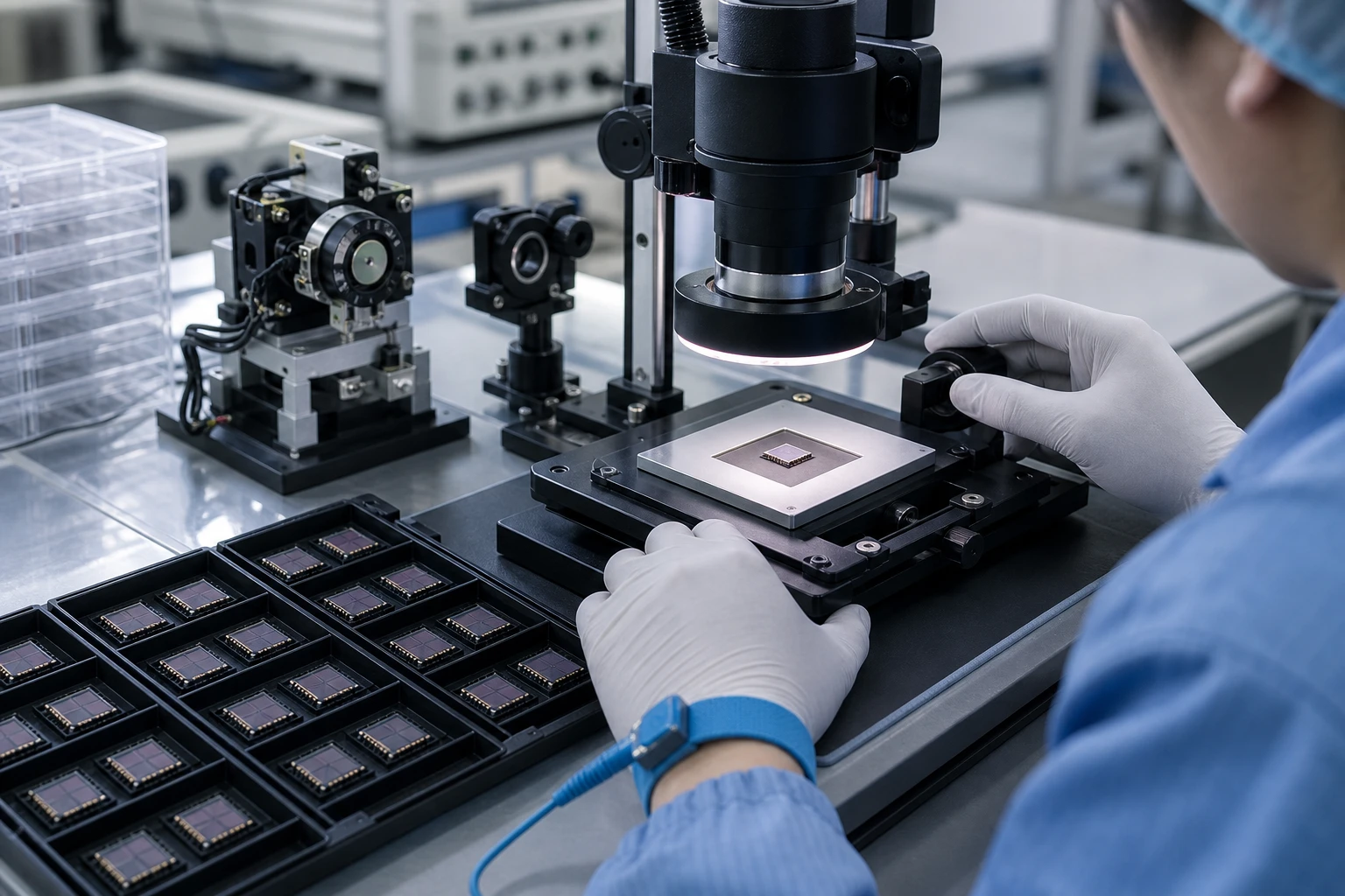
Si es ingeniero de hardware y está esbozando el diseño de su próxima placa de circuito impreso, probablemente haya llegado a ese momento en el que se pregunta: ¿debo elegir un fotodiodo de agujero pasante o uno SMD? No se trata de un detalle insignificante. La elección entre un fotodiodo SMD o un fotodiodo pasante afecta a todos los aspectos, desde el espacio en la placa y la velocidad de montaje hasta la fiabilidad a largo plazo e incluso el comportamiento del dispositivo cuando recibe el impacto de la luz. He pasado años en BeePhoton ayudando a la gente a resolver este problema y, créame, no hay una respuesta única. Pero vamos a hablar de ello como lo haríamos tomando un café, sin palabrería, sólo hablaremos de lo que realmente importa para tu diseño.
Desglose rápido: ¿Qué son exactamente los fotodiodos pasantes y SMD?
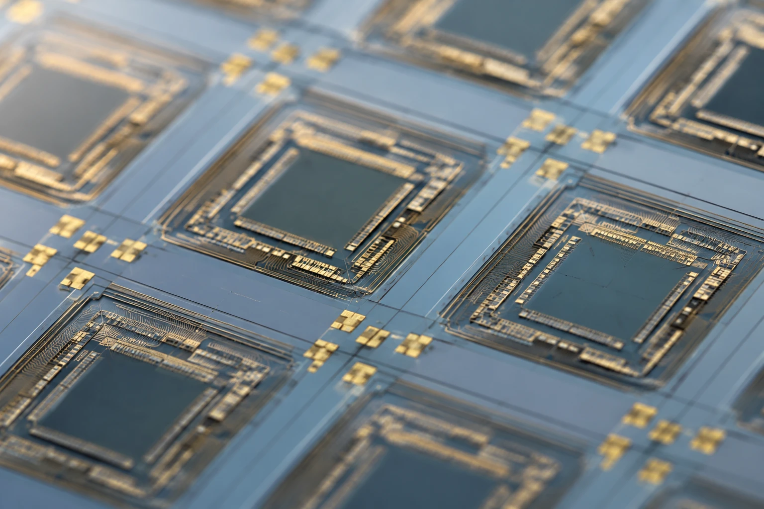
Los fotodiodos pasantes tienen los clásicos cables que atraviesan los orificios de la placa de circuito impreso. Se sueldan por el otro lado y quedan bien fijos. La diferencia entre los fotodiodos SMD y los de agujero pasante empieza aquí: las versiones de montaje superficial se saltan los agujeros por completo. Sus minúsculos contactos se asientan planos sobre almohadillas de cobre, se pegan y refluyen en una rápida pasada por el horno.
En la actualidad, ambos tipos suelen ser fotodiodos PIN de Si, ya que ofrecen una respuesta rápida, una sensibilidad decente en el visible y el infrarrojo cercano y un bajo nivel de ruido para la mayoría de los trabajos con sensores. Pero el encapsulado cambia las reglas del juego. Una pieza con orificio pasante puede venir en una lata metálica TO-18 o en una carcasa de plástico con patas más largas. Las versiones SMD caben en diminutos paquetes planos de tipo 0805 o personalizados que ahorran mucho espacio.
Por qué el embalaje es más importante de lo que cree en el fotodiodo SMD frente al fotodiodo pasante
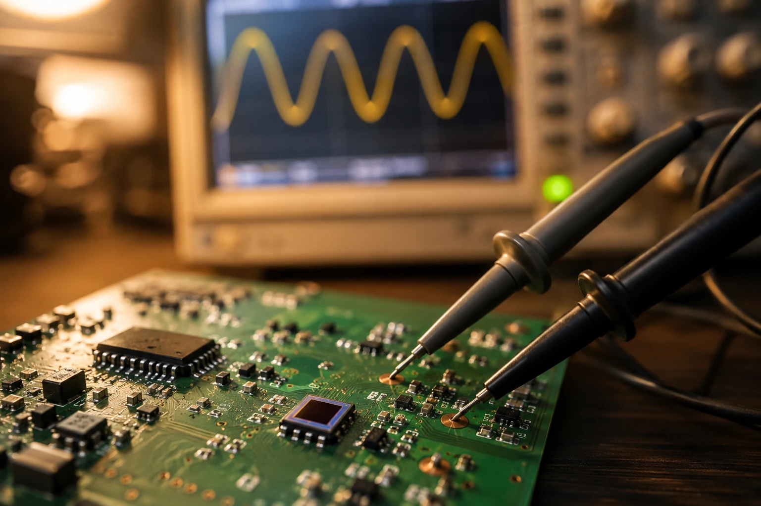
Esto es lo que la mayoría de las hojas de datos pasan por alto. El encapsulado no es sólo un envoltorio: afecta a la inductancia parásita, la capacitancia, el flujo de calor e incluso la cantidad de luz que llega realmente a la zona activa. En la detección óptica de alta velocidad, los cables más cortos de los fotodiodos SMD reducen la inductancia, lo que se traduce en señales más limpias a frecuencias de MHz. ¿Los cables largos de las piezas con orificios pasantes? Actúan como pequeñas antenas y pueden añadir ruido, especialmente por encima de unos cientos de kHz.
Por otro lado, los agujeros pasantes proporcionan un sólido anclaje mecánico. Si tu PCB va a viajar en una máquina que vibra o va a estar en un coche bajo el capó, ese agarre extra es importante. Las uniones SMD se basan principalmente en la resistencia del filete de soldadura, que está bien para la mayoría de las cosas de consumo, pero puede agrietarse bajo golpes fuertes.
Conjunto de fotodiodos PIN de Si de cuatro cuadrantes PD PDCA04-102
En busca de un alto rendimiento B2B Conjunto de fotodiodos PIN de Si para la detección de precisión? En PDCA04-102 es un detector premium de cuatro cuadrantes diseñado para aplicaciones industriales OEM. Con un robusto encapsulado de 16,5×14,5 mm y cuatro grandes elementos fotosensibles de 5×5 mm, esta matriz ofrece una consistencia y sensibilidad excepcionales para la detección de posición y los sistemas de alineación láser. Asóciese con Bee Photon para obtener una fabricación a granel fiable y soluciones personalizadas.
Comparación directa: Especificaciones de los fotodiodos SMD frente a los de agujero pasante que realmente cuentan
Se lo explicaré en una tabla sencilla para que no tenga que buscar en diez hojas de datos.
| Aspecto | Fotodiodo pasante | Fotodiodo SMD | ¿Ganador del premio al mayor número de diseños de PCB? |
|---|---|---|---|
| Tamaño y espacio del tablero | Huella más grande, necesita agujeros taladrados | 50-80% más pequeño, se adapta a ambos lados del tablero | SMD |
| Velocidad de montaje | Soldadura más lenta, a menudo manual o por ola | Recogida y colocación totalmente automatizadas, de 5 a 10 veces más rápidas | SMD |
| Resistencia mecánica | Excelente - los cables lo fijan en su sitio | Bueno, pero depende de las soldaduras | Agujero pasante |
| Rendimiento en alta frecuencia | Mayor inductancia parásita de los conductores | Menor inductancia, mejor para señales rápidas | SMD |
| Disipación del calor | Decente pero los cables pueden actuar como vías de calor | Más cerca del cobre de la placa, a menudo mejor térmico | Ligero borde a SMD |
| Prototipos y reparaciones | Súper fácil: sólo tienes que coger un soldador | Difícil sin aire caliente o estación de repaso | Agujero pasante |
| Coste a gran volumen | Mayor debido a la perforación y a un montaje más lento | Inferior - escala maravillosamente | SMD |
| Resistencia a vibraciones y golpes | Nivel superior | Sólido pero necesita un buen proceso de soldadura | Agujero pasante |
| Corriente oscura típica | Rango de nA similar (depende del troquel, no del encapsulado) | Similar, pero los paquetes más pequeños pueden funcionar más fríos | Corbata |
Cifras como la colocación entre 5 y 10 veces más rápida proceden de pruebas comparativas reales de la industria en líneas SMT frente a taladros pasantes. Y sí, un estudio del IEEE sobre la fiabilidad de los componentes mostró configuraciones SMD con alrededor de 37% menores tasas de fracaso de campo en entornos controlados - sobre todo porque la soldadura automatizada es mucho más consistente.
Cómo afecta el fotodiodo SMD frente al de agujero pasante a las cifras reales de rendimiento
Hablemos de fórmulas sin ponernos empollones. La fotocorriente que ve realmente el circuito es bastante sencilla: la fotocorriente (Iph) es igual a la capacidad de respuesta (S en A/W) por la potencia óptica incidente (P en vatios). La mayoría de los fotodiodos PIN de Si rondan entre 0,4 y 0,6 A/W en el rango visible. El tipo de encapsulado no cambia mucho la física del chip, pero sí la cantidad de luz que incide en él y la rapidez con la que se puede leer la señal.
La corriente oscura (Id), la fuga que se produce en la oscuridad, suele situarse en los nA en ambos casos. Pero en los encapsulados SMD, la menor masa térmica puede mantener la unión más fría en diseños densos, lo que en la práctica mantiene la Id más baja. La velocidad de respuesta depende de la capacitancia terminal (Cj) más la resistencia de carga. Una menor Cj en muchos diseños SMD (gracias a una geometría más ajustada) significa que se alcanzan frecuencias de corte más altas antes de que la señal se atenúe.
En un proyecto que realizamos para un sensor industrial, el cambio de fotodiodo pasante a SMD redujo el tamaño de la placa en casi 40% y nos permitió aumentar la frecuencia de muestreo en 25% gracias a la reducción de parásitos. El cliente no notó ninguna disminución de la sensibilidad; de hecho, ganó un poco gracias a un mejor acoplamiento de la luz en el encapsulado más plano.
Cuando los fotodiodos pasantes siguen teniendo sentido
No descarte los taladros pasantes sólo porque los SMD estén de moda. Si está construyendo prototipos o series pequeñas, no hay nada mejor que la facilidad de soldar a mano e intercambiar piezas sobre la marcha. En entornos hostiles, como los bajos de los automóviles, los equipos industriales de exterior o cualquier otro lugar con vibraciones constantes, el bloqueo mecánico de los taladros pasantes siempre gana. Hemos visto piezas SMD que sobreviven bien en condiciones de laboratorio, pero que empiezan a agrietarse después de seis meses de vibraciones en el mundo real de los camiones.
Además, si su diseño necesita una mayor potencia o áreas activas más grandes para recoger la luz tenue, los encapsulados con orificios pasantes suelen admitir matrices más grandes sin obligarle a realizar exóticas (y costosas) huellas SMD personalizadas.
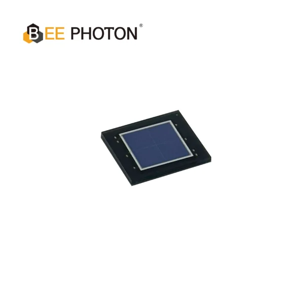
Fotodiodo PIN de Si con sensibilidad NIR mejorada (430-1100nm) PDCP08-201
En PDCP08-201 es un sistema de alto rendimiento Fotodiodo SMD Si PIN diseñado para la comunicación óptica de precisión y la detección médica[.1] Con una gran área activa de 2,9×2,9 mm, una sensibilidad NIR mejorada (0,70 A/W) y una corriente oscura ultrabaja (20 pA), este Fotodiodo SMD Si PIN garantiza una detección de señales y una fiabilidad superiores en un encapsulado compacto de montaje superficial.
Cuando los fotodiodos SMD se imponen en la selección moderna de componentes de PCB
¿Consumo de alta densidad o IoT? SMD por todos los medios. La placa es más pequeña, más ligera y más barata de fabricar a gran escala, y se pueden duplicar los componentes en ambos lados. Las líneas automatizadas los adoran: menos mano de obra, menos defectos, tiempo de comercialización más rápido. Además, para la alineación óptica en espacios reducidos, el perfil SMD plano a menudo le permite montar justo al lado de lentes o fibras sin separadores adicionales.
En BeePhoton vemos montones de proyectos de analizadores médicos portátiles y portátiles que utilizan SMD porque cada milímetro cuenta. Un cliente redujo el coste de su lista de materiales en 18% y el grosor de la placa en 30% simplemente cambiando sus fotodiodos PIN de Si por versiones de montaje superficial.
Escenarios de aplicación reales que hemos visto
Por ejemplo, el monitor ambiental compacto que estaba diseñando un cliente. El diseño original con orificios pasantes funcionaba, pero la placa era demasiado grande para la carcasa. Cambiamos a nuestros fotodiodos SMD Si PIN, los redirigimos un poco, y boom - la misma sensibilidad, la mitad de tamaño, y pasaron las pruebas de vibración con gran éxito después de un rápido ajuste del perfil de soldadura.
Otro caso: un escáner de código de barras industrial que vivía en una fábrica polvorienta. Se quedaron con los fotodiodos pasantes porque los técnicos de campo necesitaban cambiar los sensores rápidamente durante el mantenimiento. El tiempo de reparación pasó de 45 minutos a menos de 10. Diferentes necesidades, diferente ganador en el enfrentamiento entre fotodiodos SMD y fotodiodos pasantes.
Consejos rápidos para elegir el adecuado en su próxima maquetación
Empiece por sus limitaciones. ¿Poco espacio y mucho volumen? SMD. ¿Prototipos o entornos difíciles? Agujero pasante. ¿Mixto? Muchas placas son híbridas: SMD para la matriz de fotodiodos y pasante para los conectores.
Compruebe con antelación las capacidades de su taller de montaje. Algunos talleres cobran un suplemento por los pasos de taladro pasante. Consulte también la hoja de datos del fotodiodo PIN de Si que haya elegido: no todos los paquetes son iguales, ni siquiera dentro de la misma serie.
Y no te olvides de la térmica. Los diseños SMD densos pueden calentarse más en general, así que planifica tus vaciados de cobre y quizás añade un pequeño disipador térmico bajo el fotodiodo si estás utilizando una polarización inversa alta.
Conclusión sobre la elección entre fotodiodos SMD y fotodiodos pasantes
¿Cuál es mejor? Depende, pero ahora ya tiene los detalles reales en lugar de consejos genéricos. La mayoría de los diseños modernos se inclinan por el SMD por su coste, tamaño y velocidad, pero el taladro pasante sigue dominando los nichos de alta fiabilidad y prototipos. Lo más inteligente es probar ambos en el circuito de aplicación real. Ahí es donde la goma se encuentra con la carretera.
Si usted está luchando con esto ahora para su PCB, le tenemos. BeePhoton fabrica placas de Fotodiodos PIN de Si tanto en paquetes pasantes como SMD, y podemos ayudarle a especificar la combinación perfecta. Visite nuestra página de contacto o envíe un correo electrónico a info@photo-detector.com. Díganos cuáles son sus limitaciones de diseño y sus condiciones de iluminación y le enviaremos una recomendación rápida y un presupuesto el mismo día. Nada de ventas agresivas, solo ayuda honesta para que su diseño funcione en el mundo real.

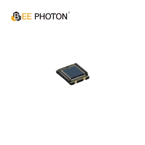
Fotodiodo PIN de Si con sensibilidad NIR mejorada (350-1100nm) PDCC100-501
Consiga resultados uniformes con nuestro diodo PIN de Si de alta consistencia para dispositivos médicos. Este fotodiodo COB proporciona una sensibilidad NIR fiable para la supervisión de la salud. Confíe en nuestro diodo PIN de Si de alta consistencia.
PREGUNTAS FRECUENTES
¿Cuál es la mayor diferencia práctica cuando se compara un fotodiodo SMD con uno de agujero pasante en una placa de circuito impreso real?
Tamaño y montaje. Las versiones SMD reducen drásticamente el tamaño de la placa y vuelan a través de las líneas automatizadas, mientras que los taladros pasantes ofrecen una resistencia mecánica a prueba de balas, pero consumen más espacio y tiempo.
¿Es siempre más fiable un fotodiodo pasante que uno SMD para aplicaciones con muchas vibraciones?
Mi experiencia me dice que sí. Los conductores fijan mejor que las almohadillas de soldadura por sí solas. Hemos visto piezas SMD que resisten tras un diseño cuidadoso, pero los agujeros pasantes tienen ese margen extra.
¿Cómo me decido entre un fotodiodo SMD o un fotodiodo pasante para un nuevo proyecto de hardware?
Haga una lista de sus prioridades: espacio en la placa, volumen de producción, necesidades de reparación y medio ambiente. A continuación, adquiera muestras de ambos productos de proveedores como BeePhoton y pruébelos en su circuito real. Los datos siempre ganan a la teoría.
¿Puedo mezclar fotodiodos SMD y de agujero pasante en la misma placa?
Por supuesto, muchos diseños hacen exactamente eso. Utilice SMD para matrices de sensores densas y agujeros pasantes cuando necesite conectores resistentes o intercambios de campo sencillos. Sólo tienes que planificar cuidadosamente el proceso de soldadura.