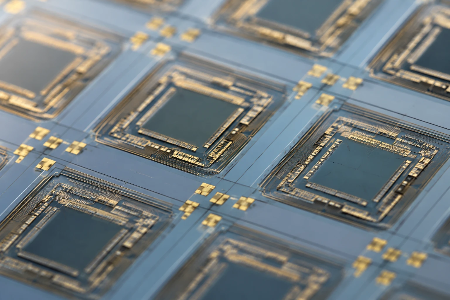
A galvanometer scanner can move quickly and accurately, but the position feedback circuit is only as reliable as its weakest part. In many designs, that weak point is not the mirror, motor, or control algorithm. It is the small optical detector sitting inside a noisy mechanical and electrical environment.
When engineers integrate a galvanometer position detector chip, they usually focus first on the photodiode’s wavelength, active area, and responsivity. Those details matter, of course. But they are only half the job. The way the bare die is bonded, the position of the optical window, the PCB return path, the transimpedance amplifier, and even the adhesive can change the final position signal.
This guide explains the practical layout rules behind a reliable galvanometer position detector chip design. It is written for hardware engineers, PCB layout engineers, optical module designers, and teams working with COB packaging photodiodes or die bonding photodetectors.
The short version is simple:
- Keep the photodiode physically close to the optical target.
- Keep the detector current path short and quiet.
- Treat the photodiode node as a high-impedance antenna.
- Separate motor and switching-current paths from the sensor return.
- Control stray light before trying to fix it in software.
- Validate the mechanical and electrical layout together, not one after another.
What Does a Galvanometer Position Detector Chip Do?
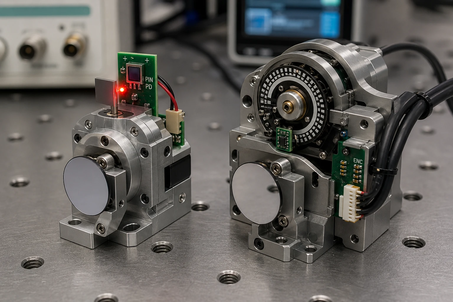
A galvanometer position detector chip is usually part of an optical feedback system. A light source projects a beam toward a moving mirror, and the reflected or redirected light reaches a photodetector. As the mirror angle changes, the amount or location of received light changes. The detector converts that optical change into a current.
The current is then converted into a voltage, commonly by a transimpedance amplifier, or TIA.
The basic relationship is:
Vout = Vref – Iphoto × Rf
Dónde:
- Vout is the amplifier output voltage.
- Vref is the reference or bias voltage.
- Iphoto is the photodiode current.
- Rf is the feedback resistor.
The minus sign depends on the photodiode polarity and amplifier configuration. In a real circuit, parasitic capacitance, amplifier input noise, feedback capacitance, and PCB leakage also affect the result.
A galvanometer position detector chip may be used in:
- Laser marking and engraving systems.
- Laser scanning modules.
- Projection engines.
- Optical barcode and imaging equipment.
- Beam steering systems.
- Medical and laboratory optical instruments.
- Industrial inspection equipment.
- Closed-loop galvo motor control.
The detector does not directly “know” the mirror angle. It measures an optical condition that correlates with the angle. That means the optical geometry and detector placement are just as important as the electrical schematic.
Why Layout Quality Matters More Than Many Teams Expect
A photodiode can generate a very small signal. Depending on optical power and device design, the useful signal may be in the microampere or nanoampere range. Meanwhile, the same assembly may contain:
- A galvanometer coil carrying rapidly changing current.
- A motor driver with PWM switching.
- A DC/DC converter.
- A laser driver.
- High-speed digital interfaces.
- Long cables between the sensor board and controller.
- Metal parts that create unpredictable return paths.
This is a bad neighborhood for a high-impedance sensor node.
A galvanometer position detector chip does not need a huge amount of noise to produce a visible error. For example, if a TIA uses Rf = 100 kΩ, an unwanted current of only 10 nA creates:
Vnoise = 10 nA × 100 kΩ = 1 mV
That 1 mV may look harmless. But if the detector output is used for fine angle correction, the error can become measurable position jitter, scan-line distortion, or unstable servo behavior.
A useful design mindset is to ask:
“Where can the unwanted current enter, and where does it return?”
That question is often more productive than simply adding a larger capacitor or increasing software filtering.
Start With the Optical and Mechanical Stack-Up
Before placing a galvanometer position detector chip on the PCB, define the complete optical stack-up. A detector that is electrically perfect can still fail if the light spot moves partly off the active area or hits the package edge during scanning.
The mechanical drawing should include:
- Galvo mirror center and rotation axis.
- Nominal beam path.
- Maximum beam angle.
- Photodiode active area.
- Detector die orientation.
- Optical stop or aperture.
- Cover glass, window, and lens locations.
- COB substrate thickness.
- Bond-wire clearance.
- Adhesive thickness.
- Thermal expansion direction.
- Service and assembly tolerances.
For a simple linear position detector, the approximate spot displacement can be estimated as:
Δx ≈ f × Δθ
Dónde:
- Δx is the lateral spot movement.
- f is the effective optical distance or focal length.
- Δθ is the angular movement in radians.
For a reflected beam from a rotating mirror, the beam angle can change by approximately twice the mirror angle:
Δθbeam ≈ 2 × Δθmirror
This is a common source of layout mistakes. An engineer may calculate the mirror movement correctly but forget that reflection doubles the beam angular change.
A practical example:
- Effective optical distance: 20 mm.
- Mirror movement: ±1°.
- Beam angular movement: approximately ±2°.
- 2° in radians: about 0.0349 rad.
- Spot movement: 20 mm × 0.0349 ≈ 0.70 mm.
If the active detector width is only 1 mm, the alignment tolerance becomes very tight. The galvanometer position detector chip may need a lens, slit, diffuser, or segmented detector arrangement instead of a simple large-area photodiode.
Fotodiodos PIN de Si para Galvo PDC-C2929
El PDC-C2929 es un chip de fotodiodo PIN de silicio de 920 nm económico. Este fotodiodo PIN de silicio de 920 nm ofrece un seguimiento estable y rentable de la posición del escáner.
Mechanical Tolerance Budget
Do not leave all alignment tolerance to the final assembly technician. Build a basic tolerance budget early.
| Error source | Typical effect | Layout response |
|---|---|---|
| Die placement offset | Changes optical zero point | Add fiducials and optical alignment marks |
| Die rotation | Creates gain or linearity error | Define orientation on the COB drawing |
| Mirror tilt error | Moves the beam off target | Reserve active-area margin |
| Adhesive shrinkage | Pulls the die during cure | Use qualified adhesive and controlled cure |
| PCB warpage | Changes optical height | Specify flatness and support points |
| Cover-window tilt | Adds beam deviation | Control window parallelism |
| Thermal expansion | Shifts the optical center | Test over the full temperature range |
| Bond-wire loop height | Can block light or touch the cover | Set a maximum loop profile |
For a galvanometer position detector chip, mechanical repeatability is often more valuable than a very tight nominal alignment on one prototype. A design that works only when manually adjusted is not production-ready.
Bare-Die Bonding and COB Packaging Rules
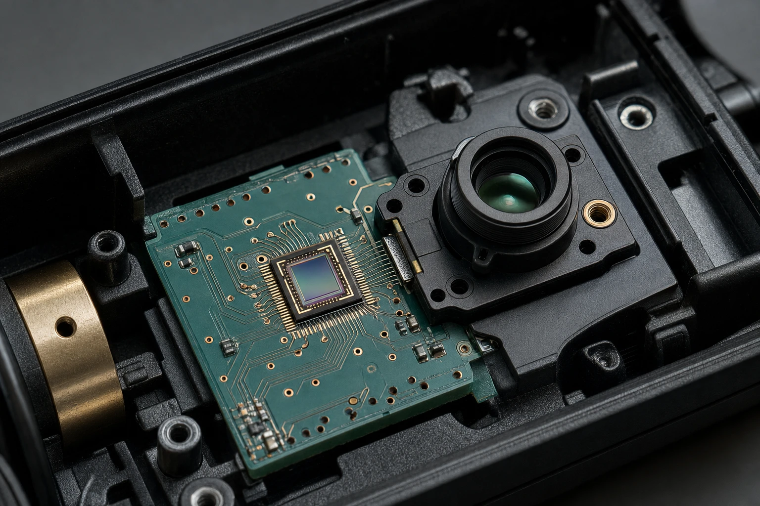
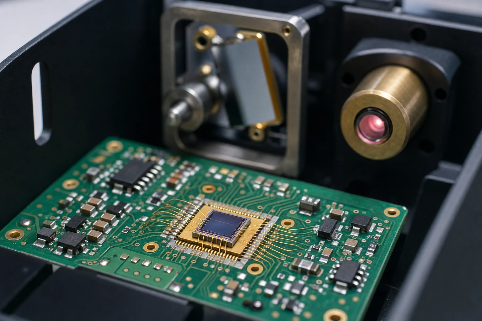
COB packaging can reduce package size and optical distance, which is helpful in a compact galvo sensor layout. It can also reduce parasitic capacitance when the die is placed close to the amplifier. But COB introduces process risks that do not appear with a standard packaged photodiode.
Define the Die Attach Surface
The die attach surface should be:
- Clean and free from oxide or residue.
- Flat enough to avoid die rocking.
- Compatible with the chosen adhesive.
- Controlled for moisture and ionic contamination.
- Designed for the required thermal path.
The adhesive layer should not spread into the active optical area. Adhesive outgassing or surface contamination near the detector can create long-term optical loss and unstable dark current.
Use a controlled dispensing pattern instead of relying on a large uncontrolled blob. The goal is to hold the die securely while keeping the active area and bond pads clean.
Keep Bond Wires Out of the Optical Path
A bond wire can reflect light, cast a small shadow, or create an unintended optical response. In a position detector, even a small obstruction can affect linearity.
The COB drawing should specify:
- Bond-wire diameter.
- Maximum loop height.
- Wire direction.
- Minimum distance from the active area.
- Minimum distance from the cover or lens.
- Bond-pad pull strength requirements.
- Encapsulation keep-out zones.
For a galvanometer position detector chip, wire direction should follow the low-noise electrical route where possible. Avoid routing a sensitive photodiode wire directly above a motor-current trace or beneath a switching node.
Choose the Encapsulant Carefully
The encapsulant or protective coating needs to match the optical wavelength and environmental conditions. Check:
- Transmission at the operating wavelength.
- Yellowing after thermal aging.
- Moisture absorption.
- Shrinkage during cure.
- Stress on the die.
- Ionic contamination.
- Compatibility with the photodiode surface.
A black optical shield can be useful for blocking ambient light, but it must not cover the intended signal path. A mechanically opaque wall or aperture is often better than coating the entire detector area with an unpredictable dark material.
Die Bonding Is Not Just an Assembly Detail
When a die bonding photodetector is placed close to a galvo motor, the substrate and adhesive can become part of the noise and thermal system. The die attach material may conduct heat, introduce stress, or create a leakage path.
During qualification, inspect the sensor after:
- Thermal cycling.
- High-humidity storage.
- Vibration.
- Repeated galvanometer movement.
- Laser on/off cycling.
- Long-duration operation at maximum optical power.
A first article that works on the bench does not prove that the COB process is stable.
Electrical Layout for a Galvanometer Position Detector Chip
The electrical layout should be designed around the photodiode current, not around the physical convenience of the connector.
Keep the Photodiode Node Very Short
The trace from the photodiode to the TIA input should be as short as practical. It should also have minimal copper area.
This node is high impedance, so it can pick up:
- Electric-field coupling from switching nodes.
- Capacitive coupling from clock traces.
- Motor-driver noise.
- Leakage from dirty PCB surfaces.
- Crosstalk from adjacent sensor channels.
Do not route the photodiode node under:
- DC/DC converter inductors.
- MOSFET drains.
- PWM gate traces.
- Crystal oscillators.
- High-speed data lanes.
- Large motor-current copper.
- Connectors carrying noisy signals.
A guard ring can help in very high-impedance designs. The guard should be driven at a voltage close to the sensitive node or at a suitable low-impedance reference, depending on the circuit topology. It should not be added automatically without checking the amplifier’s bias and leakage behavior.
Place the TIA Beside the Detector
The best general arrangement is:
- Photodiode die.
- Short bond-wire or trace connection.
- TIA input.
- Feedback resistor and capacitor.
- Low-impedance output route to the controller.
Do not place the TIA several centimeters away because the controller board has more space. A long trace adds capacitance and increases the antenna area.
The total input capacitance can be approximated as:
Cin,total = Cdiode + Copamp + Cpackage + Ctrace + Cstray
Dónde:
- Cdiode is the photodiode junction capacitance.
- Copamp is the amplifier input capacitance.
- Cpackage is the package or interconnect contribution.
- Ctrace is PCB trace capacitance.
- Cstray includes nearby copper and environmental coupling.
The TIA feedback capacitor is selected partly to keep the circuit stable with this total capacitance. A common first-order estimate for the feedback capacitor is:
Cf ≈ √(Cin,total / (2π × GBW × Rf))
This is only a starting estimate. The correct value depends on the amplifier’s input capacitance, gain-bandwidth product, phase margin, photodiode capacitance, and desired bandwidth. Always verify the result with the actual amplifier model or a measured prototype.
Use a Continuous Reference Plane, But Not Blindly
A solid reference plane near the TIA can reduce loop area and provide a controlled return path. However, placing a plane directly under every photodiode trace is not always ideal because it increases capacitance at the high-impedance input.
A useful compromise is:
- Keep the detector-to-TIA connection short.
- Avoid large ground copper around the high-impedance input.
- Use a controlled local reference near the amplifier.
- Keep the rest of the signal path over a clean, continuous plane.
- Do not split the plane underneath the TIA without a clear reason.
Many EMI problems are made worse by plane splits. The return current then takes a longer route, often passing through the exact area where the sensor is trying to measure a small signal.
Separate Analog and Motor Return Currents
The galvanometer coil return should not share a narrow trace with the photodiode or TIA return. A motor driver can create large voltage changes across a small common impedance:
Verror = Ireturn × Zcommon
Even a small shared impedance can produce a visible error. Use a deliberate star point or low-impedance power architecture, depending on the complete system design.
The exact grounding method depends on whether the system uses:
- A single supply.
- Separate analog and motor supplies.
- Isolated motor power.
- A metal chassis.
- Shielded sensor cables.
- Differential ADC inputs.
- A remote controller board.
The rule is not “always use star grounding.” The better rule is “make high-current return paths predictable and keep them away from the detector reference.”
Fotodiodos PIN de Si para Galvo PDC-2C3432-NIR-B
En PDC-2C3432-NIR-B es un especializado chip de fotodiodo PIN segmentado diseñado para una retroalimentación de posición diferencial precisa en escáneres galvanométricos de alta velocidad. La integración de este canal dual chip de fotodiodo PIN segmentado permite que los sistemas obtengan un seguimiento angular preciso con un ruido de señal mínimo.
EMI Control in a Galvo Sensor Layout
A galvo sensor layout is particularly sensitive because the actuator and detector are physically related. The motor driver may be close to the photodiode by necessity, but the current path does not need to be close.
Control the Noise at Its Source
Before adding filtering to the sensor output, reduce the noise produced by the motor driver:
- Minimize high-current loop area.
- Place ceramic decoupling capacitors close to switching devices.
- Control gate-drive slew rate when switching loss permits.
- Add snubbers only after measuring the ringing.
- Keep motor phase traces compact and paired.
- Avoid routing motor phases beside the detector input.
- Use shielded or twisted motor wiring when cables are required.
A filter on the detector output may hide some noise, but it cannot fix optical modulation, ground bounce, or amplifier saturation.
Use Shielding With a Defined Purpose
A shield should block a known coupling path. A grounded metal cover may help with electric-field interference, but it can also:
- Add parasitic capacitance.
- Create a ground loop.
- Reflect unwanted light.
- Change the optical response.
- Become noisy if connected at the wrong point.
For a galvanometer position detector chip, consider separate optical and electrical shielding:
- Optical baffle: blocks stray light.
- Metal shield: reduces electric-field coupling.
- Grounded guard: reduces leakage and surface contamination effects.
- Cable shield: controls external cable noise.
Do not assume that a shield is helpful just because it is grounded. Measure the system with the shield connected at different points and under the real motor operating condition.
Watch the Laser Driver
The laser driver can interfere with the sensor in two ways:
- Electrical coupling through power and ground.
- Optical modulation caused by laser-current ripple.
If the detector sees the same laser used for scanning, laser ripple may appear as position noise. The optical signal should be checked with the galvo stopped and with the motor driver disabled. Then repeat the measurement while enabling each noisy subsystem separately.
This simple test often shows whether the problem is electrical EMI or optical intensity variation.
Selecting the Photodiode Structure
The right detector geometry depends on the optical feedback method.
Single-Area Si PIN Photodiode
A single-area Si PIN photodiode is suitable when the optical system converts position into received intensity or when a separate optical structure creates a predictable intensity slope.
For near-infrared galvo systems, review the actual responsivity and spectral response at the laser wavelength. Do not select a detector based only on the phrase “silicon photodiode.” Silicon response changes significantly across wavelength, and the package window may also affect transmission.
BeePhoton provides product options for this type of design, including the PDC-C2928-NIR-B 940 nm Si PIN photodiode chip and the PDC-C2929 Si PIN photodiode for 920 nm applications.
Segmented PIN Photodiode
A segmented detector can provide a differential position signal. For a two-segment detector, a common normalized position signal is:
Position signal = (I1 – I2) / (I1 + I2)
Dónde:
- I1 is the current from segment 1.
- I2 is the current from segment 2.
This ratio reduces sensitivity to total optical power changes, at least in theory. It is not magic. If one segment has different responsivity, leakage, capacitance, or amplifier gain, the result will still drift.
A segmented photodiode can be useful when the beam moves across a boundary and the control system needs directional information. BeePhoton’s PDC-2C3432-NIR-B segmented PIN photodiode chip may be relevant for this type of architecture. Confirm the available die drawings, active-area dimensions, spectral response, and electrical limits before finalizing the COB layout.
| Detector approach | Main benefit | Main risk | Layout focus |
|---|---|---|---|
| Single-area PIN | Simple circuit and compact assembly | Sensitive to laser power variation | Stable optical slope and low-noise TIA |
| Segmented PIN | Differential position information | Channel mismatch and extra capacitance | Matched routing and matched amplifier channels |
| Multiple discrete detectors | Flexible optical geometry | Larger mechanical stack-up | Consistent alignment and thermal tracking |
| Packaged photodiode | Easier handling | Larger parasitics and height | Package clearance and short interconnect |
| Bare-die detector | Compact COB integration | Assembly and contamination risk | Die placement, bonding, and process control |
Matched Routing for Segmented Detectors
When using a segmented galvanometer position detector chip, treat the two channels as a matched analog pair.
Try to match:
- Bond-wire length.
- PCB trace length.
- Trace width.
- Via count.
- TIA component values.
- Ground environment.
- Thermal surroundings.
- Optical exposure.
- Connector path.
Do not route one channel beside a motor phase and the other beside a quiet ground region. The circuit may pass a schematic review but still show position offset or noise imbalance.
For the differential calculation, use enough signal headroom. If I1 + I2 becomes very small, the normalized result becomes noisy because the denominator is small. Add a valid operating range or signal-present check in the control firmware.
You may also need offset calibration:
Position corrected = measured position – electrical offset – optical offset
The optical offset can come from die placement, mirror angle, lens centering, or the detector segment boundary. Calibrate the complete module, not only the bare PCB.
TIA Component Placement and Stability
The feedback resistor should be directly beside the amplifier feedback pins. The feedback capacitor should have the smallest practical loop area.
Avoid placing the feedback network across a noisy region or routing other signals through the TIA feedback loop. The amplifier input, feedback resistor, and feedback capacitor should form a compact group.
The approximate TIA bandwidth is:
f-3dB ≈ 1 / (2π × Rf × Cf)
This is a simplified estimate and should not be treated as the complete closed-loop response. It is useful for checking whether a chosen feedback capacitor is in the right general range.
A larger Rf gives more voltage gain but reduces overload margin and usually requires more attention to stability. A smaller Rf increases headroom but may reduce sensitivity.
Use this basic check:
Vout,max = Iphoto,max × Rf
Then include:
- Ambient-light current.
- Laser maximum power.
- Reflection peaks.
- Startup overshoot.
- Motor-induced transients.
- Amplifier output swing limits.
A position detector that saturates for a few microseconds may still create visible servo artifacts, especially if the controller interprets the recovery edge as a real position change.
Fotodiodos PIN de Si para Galvo PDC-C2928-NIR-B
Optimice el escaneo con nuestro chip fotodiodo PIN de 940 nm, PDC-C2928-NIR-B. Este chip fotodiodo PIN de 940 nm garantiza una detección precisa de la posición del galvanómetro y un bajo nivel de ruido.
PCB Material, Cleanliness, and Leakage
At low photodiode currents, PCB cleanliness can become a real electrical issue. Flux residue, dust, moisture, and fingerprints can create leakage paths around the TIA input.
Useful production controls include:
- A validated cleaning process.
- Controlled no-clean flux selection.
- High-impedance inspection after assembly.
- Protective coating only after checking parasitic effects.
- Keep-out areas around the detector input.
- Avoiding unnecessary vias near sensitive nodes.
A conformal coating may reduce moisture-related leakage, but it can also add capacitance and trap contamination. Test it as part of the actual design.
The galvanometer position detector chip itself may be perfectly stable while the surrounding board causes the drift.
Common Integration Mistakes
Placing the Detector Near the Connector
This often makes the assembly convenient, but it creates a long sensitive route. Put the detector and TIA near the optical point. Move the connector or digitize the signal later if needed.
Sharing the Sensor Ground With the Motor Return
This can create position error that changes with motor current. Use a planned return structure rather than joining grounds wherever copper happens to be available.
Ignoring Stray Light
A dark room test may look fine, while the final product fails under sunlight, nearby indicators, or internal laser reflections. Test with the actual cover, housing, labels, adhesives, and cables installed.
Using Software to Fix a Mechanical Problem
Calibration can remove a stable offset. It cannot reliably fix a beam that leaves the active area, a loose die, or a cover window that moves under vibration.
Choosing a Photodiode by Wavelength Name Alone
“920 nm” or “940 nm” does not describe the whole device. Review active area, capacitance, dark current, responsivity, reverse-bias limits, die dimensions, and assembly recommendations.
Forgetting the Bare-Die Drawing
The electrical symbol is not enough for COB work. You need pad dimensions, pad pitch, die thickness, orientation, keep-out areas, and any recommended bonding conditions.
A Practical Validation Plan
A reliable galvanometer position detector chip design should be tested in layers.
Optical Tests
Measure:
- Detector output versus mirror angle.
- Linearity across the operating range.
- Response with laser power variation.
- Ambient-light sensitivity.
- Optical zero-point repeatability.
- Response after cover and housing installation.
Electrical Tests
Measure:
- Dark output.
- TIA noise with the laser off.
- TIA noise with the laser on.
- Output during motor startup.
- Output during maximum motor acceleration.
- Supply ripple sensitivity.
- Ground potential difference between sensor and controller.
EMI Tests
Run the test under several conditions:
| Test condition | What it helps identify |
|---|---|
| Laser off, motor off | Electrical baseline |
| Laser on, motor off | Optical and laser-driver noise |
| Laser off, motor on | Motor EMI and ground bounce |
| Laser on, motor on | Real operating condition |
| Shield connected at sensor end | Cable and electric-field coupling |
| Shield connected at controller end | Ground-loop and return-path effects |
| Shield connected at both ends | Chassis-current behavior |
| Cover installed | Internal reflection and mechanical effects |
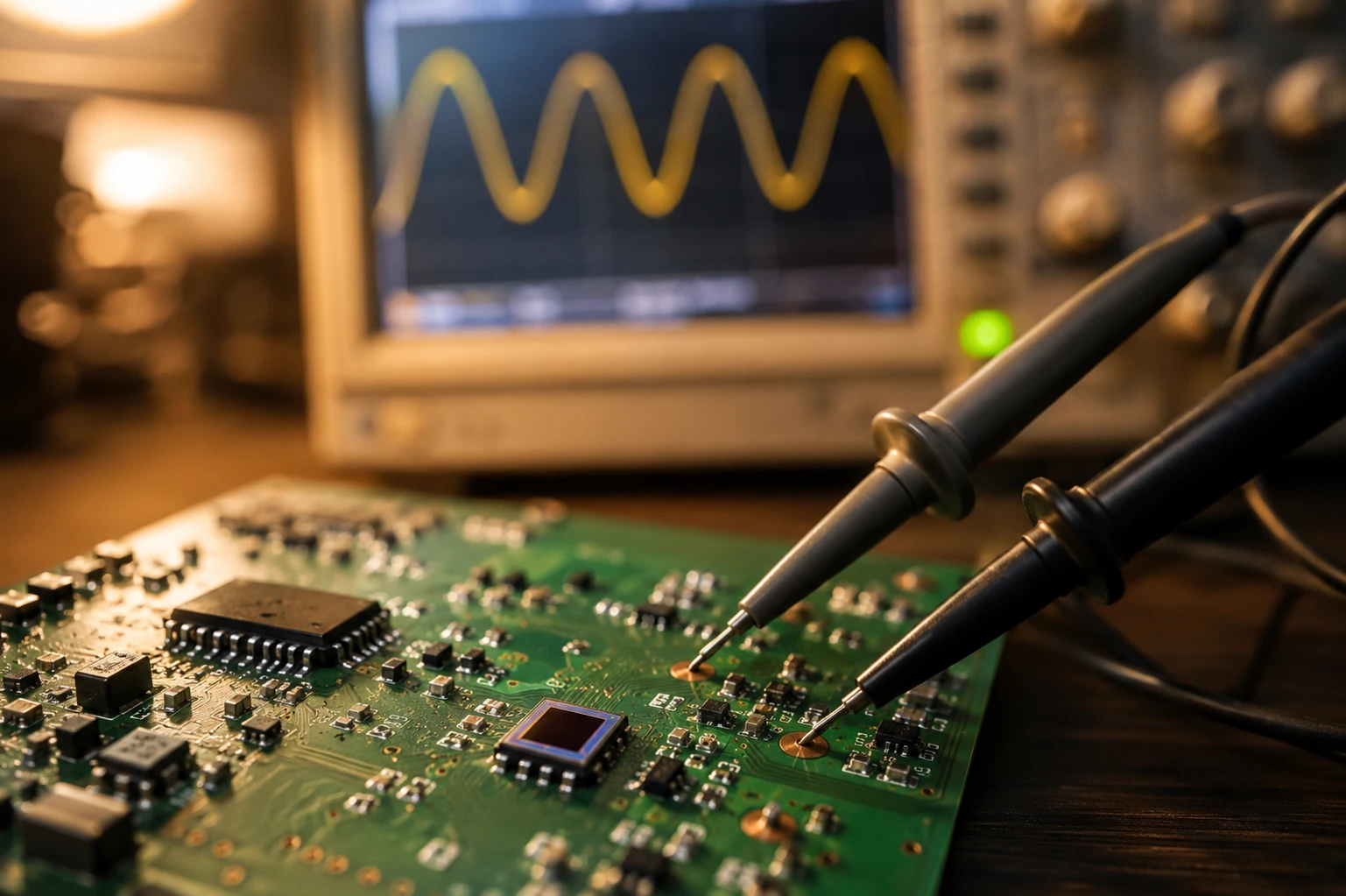
Record the detector output with an oscilloscope before adding digital filtering. Save the raw waveform. A filtered graph can make a poor layout look acceptable for a short test.
Environmental Tests
Include:
- Temperature sweep.
- Humidity exposure.
- Vibration.
- Mechanical shock where applicable.
- Repeated power cycling.
- Long-duration laser operation.
- Long-duration galvo scanning.
For COB assemblies, inspect optical alignment and bond integrity after testing. The electrical signal may still work while the gain or offset has slowly moved.
How BeePhoton Can Support the Design
Choosing a galvanometer position detector chip is not only a catalog exercise. The die must fit the optical geometry, bonding process, current range, and PCB strategy.
When comparing devices, prepare these questions:
- What are the die dimensions and pad locations?
- What active-area geometry is available?
- What wavelength range matches the laser?
- What is the expected photocurrent?
- What is the junction capacitance?
- Is the die suitable for COB packaging?
- What bond-wire and encapsulation limits apply?
- Is a segmented structure better than a single-area detector?
- Can samples be supplied for optical and EMI testing?
- What customization or technical support is available?
You can review BeePhoton’s 940 nm Si PIN photodiode option, 920 nm Si PIN photodiode option, y segmented PIN photodiode option according to your optical design.
If your team already has the mechanical drawing, laser wavelength, target scan angle, approximate photocurrent, and TIA gain, send those details through the Página de contacto de BeePhoton. You can also email info@photo-detector.com to ask about samples, bare-die bonding information, and a quotation.
A small amount of design discussion before layout can prevent several expensive COB revisions later.
Final Design Checklist
Before releasing the galvanometer position detector chip layout, check the following:
- The detector active area remains covered by the beam across the full scan range.
- Reflection geometry has been calculated using the actual mirror movement.
- The die orientation is marked on the COB drawing.
- Bond wires do not cross the optical path.
- Adhesive does not spread into the active area.
- The TIA is close to the detector.
- The photodiode input trace is short and compact.
- No switching node or motor phase runs beside the input.
- Motor return current does not share the sensor return path.
- The feedback resistor and capacitor are beside the TIA pins.
- Total input capacitance has been estimated.
- TIA stability has been checked with the real detector and layout.
- Stray light has been tested with the final housing.
- Segmented channels are routed and loaded symmetrically.
- The circuit does not saturate at maximum optical power.
- PCB cleanliness and moisture leakage have been considered.
- Samples have been tested under real motor operation.
- Calibration limits are defined before production.
PREGUNTAS FRECUENTES
¿Cuál es la mejor ubicación en la PCB para un chip detector de posición de galvanómetro?
Coloque el chip detector de posición del galvanómetro lo más cerca posible del objetivo óptico y del amplificador de transimpedancia. La conexión entre el detector y el TIA debe ser corta, directa y estar aislada de las fases del motor, trazas de PWM, reguladores de conmutación y señales digitales de alta velocidad. La ruta de retorno del sensor también debe planificarse de forma independiente a los retornos del motor de alta corriente.
¿Se puede utilizar un die de fotodiodo desnudo en el encapsulado COB?
Sí, un chip de fotodiodo desnudo puede integrarse en un encapsulado COB siempre que el sustrato, el adhesivo, el proceso de unión, el encapsulante, la ventana óptica y los controles de contaminación sean adecuados. Los planos del chip y los requisitos de unión deben revisarse antes de diseñar el sustrato COB. El espacio libre del área activa y la altura del hilo de unión son especialmente importantes en los conjuntos de retroalimentación óptica.
¿Debería utilizar un fotodiodo de área única o uno segmentado para la retroalimentación del galvo?
Un fotodiodo de área única resulta más sencillo cuando el diseño óptico convierte la posición en intensidad. Un fotodiodo segmentado puede proporcionar información de posición diferencial y puede reducir la sensibilidad a las variaciones de la potencia total del láser. Sin embargo, los canales segmentados requieren disposiciones eléctricas y ópticas adaptadas, una calibración minuciosa y una señal suficiente en ambos segmentos.
¿Cómo puedo reducir la interferencia electromagnética (EMI) en el diseño de un sensor galvanométrico?
Comience reduciendo el ruido en la fuente del controlador del motor. Minimice el área del bucle de alta corriente, coloque capacitores de desacoplamiento cerca de los dispositivos de conmutación, mantenga las pistas del motor alejadas de la entrada del fotodiodo y proporcione una ruta de retorno predecible. Luego, pruebe el blindaje óptico, el blindaje del cable y la conexión a tierra local por separado. Añadir un filtro sin encontrar la ruta de acoplamiento a menudo solo oculta el problema.
¿Qué información debo proporcionar al solicitar una cotización de fotodiodos?
Proporcione la longitud de onda del láser, la potencia óptica esperada, el ángulo de escaneo, el tamaño del haz, los requisitos del área activa del detector, la fotocorriente aproximada, la ganancia del TIA, la temperatura de funcionamiento, las dimensiones del paquete COB y el volumen anual previsto. Un dibujo mecánico o un esquema óptico también resultan útiles. Esta información ayuda al proveedor a recomendar un chip detector de posición para galvanómetro más adecuado en lugar de ofrecer una pieza genérica.
Need Help With Your Galvo Sensor Design?
A stable position feedback system comes from the whole chain: optical geometry, die bonding, COB packaging, PCB routing, grounding, shielding, and calibration. If one part is treated as an afterthought, the final signal can become noisy or drift under real operating conditions.
BeePhoton can help you compare Si PIN photodiodes and segmented detector options for galvanometer applications. Visit the product selection pages to review suitable detector categories, or contact BeePhoton for technical consultation and pricing.
Share your wavelength, optical layout, target signal range, and packaging requirements. With those details, you can move from a rough detector choice to a practical design that is easier to assemble, test, and scale.