A scanner prototype can look perfect on the engineering bench and still become a calibration headache when monthly production reaches thousands of units.
The usual complaint from QA sounds something like this:
“Every scanner passes, but the calibration values keep moving from batch to batch.”
That problem is rarely caused by one obviously defective component. More often, small variations in photodiode sensitivity, segment balance, optical alignment, amplifier gain, wavelength, temperature, and test fixtures stack together. The result is unstable retroalimentación de posicionamiento del escáner óptico, longer calibration cycles, wider parameter storage ranges, and a rather uncomfortable amount of rework.
For production engineers, the goal should not be to calibrate away unlimited variation. The better goal is to make the optical feedback chain predictable before final calibration begins.
This guide explains how to improve retroalimentación de posicionamiento del escáner óptico consistency through better photodiode specifications, measurement system analysis, incoming inspection, statistical process control, and supplier lot management. It is written for QA teams, galvo scanner manufacturers, sourcing engineers, and production managers dealing with scanner sensor batch consistency.
Why Optical Scanner Positioning Feedback Changes Between Batches
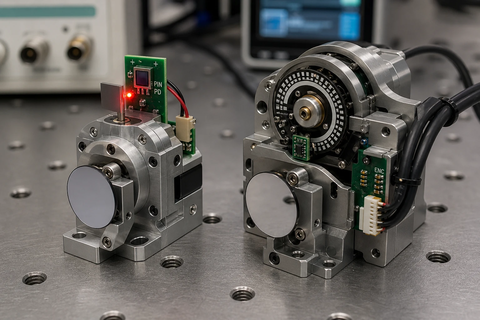
In a typical galvanometer scanner, a reflected or interrupted light beam falls on a silicon PIN photodiode, dual-element photodiode, or segmented detector. As the mirror rotates, the light spot moves across the active area. The detector converts that movement into photocurrent, and the electronic circuit turns the current into a position signal.
That sounds simple. In production, it is not.
The final retroalimentación de posicionamiento del escáner óptico signal depends on the complete measurement chain:
| Variation source | What changes | Typical production symptom |
|---|---|---|
| Photodiode responsivity | Photocurrent at a given optical power | Different feedback amplitude between lots |
| Segment sensitivity balance | Current ratio between detector sections | Center position offset or nonlinear response |
| Dark current and amplifier offset | Zero-light electrical output | Calibration zero drifts |
| Laser or LED wavelength | Detector conversion efficiency | Sensitivity changes after emitter substitution |
| Optical power | Total photocurrent | Position slope appears higher or lower |
| Beam size and shape | Light distribution across segments | Different linear range and center slope |
| Die placement | Detector location relative to the beam | Mechanical centering time increases |
| Detector angle | Effective illuminated area and reflection | Asymmetric response |
| Transimpedance gain | Current-to-voltage conversion | Detector variation is confused with PCB variation |
| Temperatura | Detector and amplifier characteristics | Warm and cold calibration values disagree |
| Test fixture repeatability | Measured value changes without a product change | Good lots appear inconsistent |
| Surface contamination | Local optical loss or scattering | Irregular signal and poor repeatability |
The annoying part is that each item may still be “within specification.” The combined system, though, may no longer deliver consistent retroalimentación de posicionamiento del escáner óptico.
That is why checking only the detector’s typical sensitivity is not enough.
How Silicon PIN Optical Feedback Produces a Position Signal
A silicon PIN photodiode generates photocurrent approximately proportional to the optical power reaching its active area:
Photocurrent = Responsivity × Incident optical power
Or, using symbols:
Iph = Rλ × P
Dónde:
- Iph is photocurrent, usually measured in amperes.
- Rλ is responsivity at a specified wavelength, usually measured in A/W.
- P is incident optical power in watts.
For a segmented detector, the position signal is often calculated from the difference between two photocurrents.
For a left-right detector:
Normalized X position = (IR − IL) ÷ (IR + IL)
Dónde:
- IR is the right-segment photocurrent.
- IL is the left-segment photocurrent.
- IR + IL represents total detected light.
- IR − IL represents the movement direction and magnitude.
For a four-segment detector, a similar calculation can be applied in both X and Y directions:
Normalized X = (Iright − Ileft) ÷ Itotal
Normalized Y = (Itop − Ibottom) ÷ Itotal
Normalization reduces the effect of total optical power changes. It does not eliminate every source of variation. Segment responsivity mismatch, beam profile changes, clipping, spot-size variation, amplifier offset, and optical misalignment can still alter retroalimentación de posicionamiento del escáner óptico.
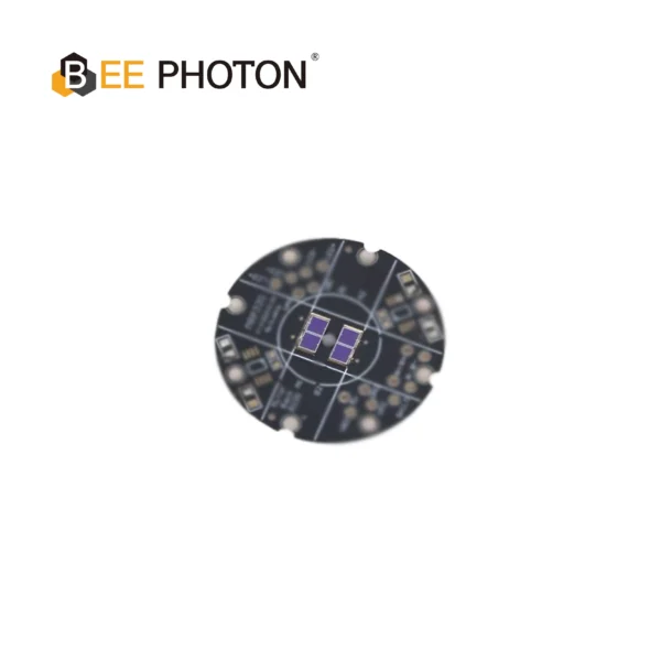
Fotodiodos PIN de Si para Galvo PDC-C2928-NIR-B
Optimice el escaneo con nuestro chip fotodiodo PIN de 940 nm, PDC-C2928-NIR-B. Este chip fotodiodo PIN de 940 nm garantiza una detección precisa de la posición del galvanómetro y un bajo nivel de ruido.
Why Normalization Does Not Fix Batch Inconsistency
There is a common assumption that dividing by total current makes detector sensitivity irrelevant. That is only partly true.
If every segment changes by exactly the same percentage, the normalized position may remain stable. Real detector lots are not always that neat. One segment may shift slightly more than another, or the sensitivity distribution across the active area may change.
Por ejemplo:
- Left-segment sensitivity increases by 2%.
- Right-segment sensitivity increases by 5%.
- Total current remains acceptable.
- The electrical center moves because the two segments no longer track equally.
The scanner can still pass a basic photocurrent test while its retroalimentación de posicionamiento del escáner óptico center and slope have changed.
For that reason, mass-production specifications should cover both total sensitivity and segment matching.
Define “Consistency” Before Asking a Supplier to Improve It
“Better consistency” is too vague for a drawing, purchase specification, or supplier corrective action request.
QA and engineering teams should convert retroalimentación de posicionamiento del escáner óptico into measurable characteristics. At minimum, define the following:
1. Total Responsivity or Photocurrent
Measure the total detector output under a controlled wavelength, optical power, spot size, position, temperature, and reverse-bias condition.
Do not specify photocurrent without specifying the illumination setup. A number measured at 920 nm cannot be casually compared with a number measured at 940 nm.
2. Segment Matching
A simple segment-matching calculation is:
Segment mismatch = |I1 − I2| ÷ ((I1 + I2) ÷ 2) × 100%
For a multi-segment positioning chip, calculate both adjacent-segment and opposite-segment mismatch where relevant.
Segment matching can affect the zero point, linearity, and calibration range of retroalimentación de posicionamiento del escáner óptico.
3. Position Sensitivity
Position sensitivity describes how much the electrical output changes for a known beam movement or mirror angle change:
Position sensitivity = Change in output ÷ Change in position
Examples include:
- V/mm at the detector plane
- Normalized output per millimeter
- V/degree of mirror rotation
- ADC counts per commanded position step
Use the unit that connects directly with your production calibration process.
4. Zero Offset
Measure the feedback output at the defined optical center. This should include a clear centering method rather than an operator’s visual judgement.
5. Linearity
One practical calculation is:
Linearity error = Maximum deviation from the fitted line ÷ Full-scale output × 100%
State the evaluation range. A detector may have excellent linearity near the center but a larger error close to the active-area boundary.
6. Lot-to-Lot Variation
For a measured characteristic such as position sensitivity:
Coefficient of variation = Standard deviation ÷ Mean × 100%
The coefficient of variation, or CV, is useful when comparing lots with different average values. However, CV should not replace minimum and maximum limits. A tightly grouped lot can still be centered on the wrong target.
Start With the Measurement System, Not the Photodiode Supplier
Before rejecting a detector lot, prove that the test setup can distinguish a real lot difference from measurement noise.
This is the point where many investigations go sideways. Engineers compare two lots, see a 2% shift, and blame the detector. Later, they discover that the test laser warmed up differently or the fixture placed the PCB 0.15 mm off center.
A basic measurement system analysis for retroalimentación de posicionamiento del escáner óptico should include repeatability, reproducibility, stability, and bias.
Repeatability
One operator measures the same sample repeatedly without changing the setup.
If the readings move too much, inspect:
- Light-source warm-up time
- Optical power stability
- Fixture clamping force
- Electrical contact resistance
- Ambient light shielding
- Detector temperature
- ADC filtering
- Beam-centering procedure
Reproducibility
Different operators or stations measure the same samples.
Large operator-to-operator differences often point to an unclear alignment method. Manual “adjust until the waveform looks centered” instructions are not a controlled process.
Estabilidad
Measure a golden sample over time. Plot the result rather than storing it in a spreadsheet nobody opens.
A golden detector or scanner assembly can reveal gradual changes in:
- Light-source output
- Fixture alignment
- Lens contamination
- Amplifier gain
- Reference power-meter calibration
- Software processing
Bias and Traceability
Where practical, reference instruments should have calibration traceable through an unbroken chain of calibrations, with uncertainty considered at each step. This follows the general approach described in the NIST policy on metrological traceability.
For uncertainty evaluation, the JCGM Guide to the Expression of Uncertainty in Measurement remains a widely accepted reference.
This does not mean every production station needs a laboratory-grade power meter attached all day. It means the station needs a known relationship to a controlled reference.
Build a Golden Optical Feedback Test Station
A reliable test station should control the variables that have the biggest effect on retroalimentación de posicionamiento del escáner óptico.
Control the Wavelength
Silicon PIN photodiode responsivity depends on wavelength. Record the actual emitter wavelength range, not just a broad label such as “near infrared.”
If production may use both 920 nm and 940 nm emitters, qualify the detector and feedback circuit under both conditions. Do not assume the difference will disappear after normalization.
Monitor Optical Power
Use a reference detector or calibrated power meter to monitor source output. If the source power changes during the test, compensate for it or stop the measurement.
For normalized differential measurements, total current is still useful. A falling total-current value may reveal contamination, beam clipping, poor die placement, or source ageing.
Fix the Beam Geometry
Specify:
- Spot diameter at the detector plane
- Beam shape
- Angle of incidence
- Working distance
- Scan path
- Centering reference
- Allowed fixture tolerance
A detector tested with a broad Gaussian spot may behave differently from one tested with a narrow or partially clipped beam.
Control Temperature
Choose a reference temperature and a realistic stabilization time. If the scanner operates across a wide temperature range, test selected samples at relevant hot and cold conditions.
Avoid touching a bare detector or nearby fixture immediately before a precision reading. Body heat can produce a small but real shift. Sounds trivial, but it causes surprisingly messy data.
Lock the Signal-Processing Method
Filtering, ADC sampling, averaging, and firmware calculations must stay consistent. A firmware revision can change apparent retroalimentación de posicionamiento del escáner óptico even when the optical hardware is identical.
Record the firmware version, gain setting, filter parameters, and calibration algorithm with every characterization report.
Use a Practical Incoming Inspection Plan
Testing every detector at full scanner level may be too slow. Testing nothing beyond supplier paperwork is risky. A layered incoming plan usually works better.
| Inspection level | Suggested check | Purpose |
|---|---|---|
| Lot documentation | Lot number, wafer or production traceability, quantity, date | Prevent mixed or unidentified material |
| Visual inspection | Surface contamination, edge damage, bond-area condition | Catch handling and packaging defects |
| Fast electrical screening | Dark current, leakage, continuity where applicable | Remove obvious electrical defects |
| Controlled optical test | Total photocurrent and segment balance | Monitor silicon PIN optical feedback |
| Sample position scan | Center offset, slope, linearity | Predict optical scanner positioning feedback |
| Golden-unit comparison | Same setup and reference detector | Separate fixture drift from lot variation |
| Production correlation | Compare incoming data with final calibration values | Confirm the incoming test predicts real assembly behavior |
Sampling plans may be based on the company’s risk level and quality agreement. ISO 2859-1 is commonly used for acceptance sampling by attributes, but it should not be treated as a magic shield. AQL sampling cannot guarantee that every unit in a lot meets a continuous sensitivity requirement.
For critical retroalimentación de posicionamiento del escáner óptico characteristics, variable data and process capability are often more informative than simple pass/fail counts.
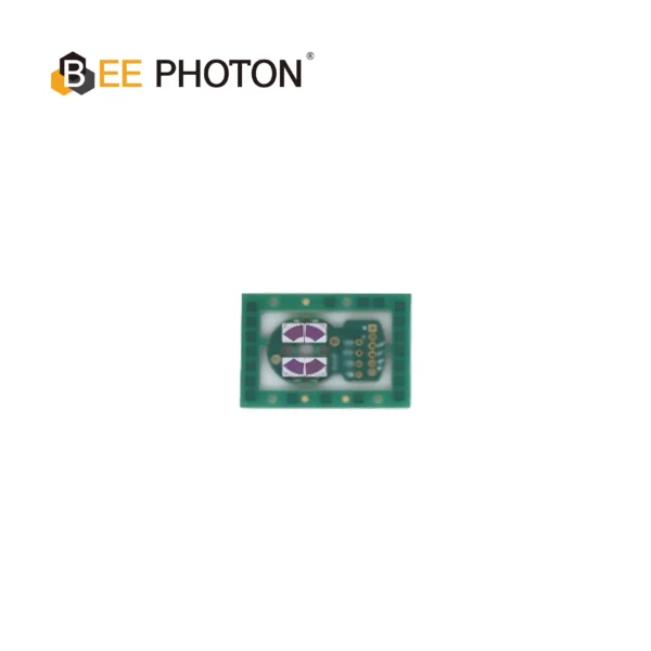
Fotodiodos PIN de Si para Galvo PDC-2C3432-NIR-B
En PDC-2C3432-NIR-B es un especializado chip de fotodiodo PIN segmentado diseñado para una retroalimentación de posición diferencial precisa en escáneres galvanométricos de alta velocidad. La integración de este canal dual chip de fotodiodo PIN segmentado permite que los sistemas obtengan un seguimiento angular preciso con un ruido de señal mínimo.
Apply SPC to Scanner Sensor Batch Consistency
Statistical process control helps distinguish common process variation from an actual process shift.
En NIST/SEMATECH Engineering Statistics Handbook provides practical guidance on control charts, measurement processes, process capability, and experimental design.
Useful charts for retroalimentación de posicionamiento del escáner óptico include:
- X-bar and R charts for subgrouped position sensitivity
- Individuals and moving-range charts for low-volume lots
- Histograms by detector lot
- Box plots comparing suppliers or wafer lots
- Scatter plots of total photocurrent versus calibration gain
- Scatter plots of segment mismatch versus center offset
Do not mix several detector lots into one chart and then calculate a single capability value. That can hide the exact batch shift you are trying to find.
Capability Calculations
When the process is stable and approximately suitable for capability analysis:
Cp = (USL − LSL) ÷ (6 × standard deviation)
Cpk = Minimum of:
(USL − mean) ÷ (3 × standard deviation)
y
(mean − LSL) ÷ (3 × standard deviation)
Dónde:
- USL is the upper specification limit.
- LSL is the lower specification limit.
- Mean is the process average.
- Standard deviation represents process spread.
Cpk should not be used as decoration in a supplier presentation. If the measurement system is poor or the process is unstable, the number can be quite misleading.
Separate Detector Variation From Assembly Variation
A fast way to waste weeks is to call every final calibration shift a “photodiode sensitivity problem.”
Use a swap test.
- Select detectors from a low-output lot and a high-output lot.
- Measure them on the same optical fixture.
- Assemble selected samples using the same PCB and mechanical setup.
- Swap detectors between assemblies where the design permits.
- Compare the change in retroalimentación de posicionamiento del escáner óptico.
- Repeat the test with the light source, amplifier board, and mechanical carrier.
If the shift follows the detector, investigate photodiode responsivity, segment balance, die geometry, or packaging. If it stays with the assembly, the cause may be optical alignment, gain tolerance, soldering stress, or firmware.
A designed experiment can go further. Detector lot, emitter lot, amplifier lot, fixture, and temperature can be treated as separate factors. Even a small, carefully planned experiment is often more useful than hundreds of unstructured measurements.
Set Better Photodiode Purchasing Specifications
A nominal wavelength and typical sensitivity value do not provide enough control for mass production.
A useful purchasing specification for a positioning photodiode should consider:
- Responsivity or photocurrent minimum and maximum
- Test wavelength and wavelength tolerance
- Optical power at the detector
- Spot size and beam position
- Reverse-bias condition
- Temperatura
- Segment-to-segment sensitivity mismatch
- Dark current limit
- Active-area geometry
- Gap dimensions for segmented devices
- Die dimensions and placement references
- Packaging and surface-protection requirements
- Lot traceability
- Change-notification requirements
- Agreed sampling or screening method
- Data format supplied with each lot
Para retroalimentación de posicionamiento del escáner óptico, average sensitivity is rarely the whole story. A tighter segment-matching requirement may reduce calibration time more effectively than an unnecessarily narrow total-responsivity limit.
That view can be controversial with purchasing teams because tighter limits may increase component cost. Still, the cheapest detector is not cheap if every scanner needs another three minutes of alignment.
Use Binning When One Universal Calibration Range Is Too Wide
If detector production naturally forms several stable sensitivity groups, binning may be more practical than demanding an unrealistically narrow distribution.
Possible bins include:
- Total photocurrent range
- Position sensitivity range
- Segment mismatch range
- Center-offset range
- Dark-current range
Production can then load the correct gain setting, resistor option, or initial calibration profile for each bin.
Binning works only when:
- The supplier’s measurement correlates with the customer’s measurement.
- Bin boundaries are documented.
- Bins are physically and electronically traceable.
- Mixed-bin packaging is prevented.
- Firmware uses the correct bin information.
Otherwise, binning just moves the confusion from the calibration station to the warehouse.
Selecting a Silicon PIN Positioning Chip for Galvo Scanners
BeePhoton offers several silicon PIN photodiode options intended for optical positioning and galvo-related applications. Device selection should begin with wavelength, active-area geometry, segment structure, optical layout, and required feedback range.
En PDC-C2929 920 nm silicon PIN photodiode can be evaluated for systems using a near-infrared optical source around the stated product wavelength. For projects centered around 940 nm, review the PDC-C2928-NIR-B photodiode chip.
Applications requiring a segmented sensing structure can also assess the PDC-2C3432-NIR-B segmented PIN photodiode chip.
Do not choose a detector from wavelength alone. Before approving a PDC-C2929 positioning chip or another device for retroalimentación de posicionamiento del escáner óptico, confirm:
- Actual emitter wavelength distribution
- Required active area
- Expected spot size
- Segment layout
- Electrical bias
- Maximum optical power
- Amplifier topology
- Temperatura de funcionamiento
- Bare-die assembly capability
- Required sensitivity distribution
- Lot-level testing and traceability
A sample evaluation should use the real scanner optics whenever possible. A benchtop illumination test is useful for screening, but it cannot fully reproduce beam movement, reflections, clipping, or assembly tolerances.
A Worked Example of Lot Comparison
The following numbers are illustrative only. They are not published performance data for a BeePhoton product or a customer production result.
Suppose a QA team measures normalized position sensitivity for two detector lots.
| Item | Lot A | Lot B |
|---|---|---|
| Sample size | 30 | 30 |
| Mean sensitivity | 0.820 per mm | 0.779 per mm |
| Standard deviation | 0.012 per mm | 0.013 per mm |
| CV | 1.46% | 1.67% |
| Mean center offset | 0.006 | 0.021 |
Both lots have relatively tight internal distributions, but their means are different.
The mean sensitivity shift is:
Sensitivity shift = (0.779 − 0.820) ÷ 0.820 × 100%
Sensitivity shift = −5.0%
This is a batch-centering issue, not simply excessive within-lot spread. Increasing final calibration limits may allow both lots to pass, but it does not improve retroalimentación de posicionamiento del escáner óptico consistency.
The next investigation should compare:
- Supplier optical test conditions
- Segment responsivity data
- Wafer or manufacturing lot
- Emitter power and wavelength
- Fixture alignment
- Assembly placement
- Amplifier gain
- Calibration firmware
The correct action might be supplier process centering, customer-side binning, or a revised gain architecture. The data should decide.
Reduce Calibration Time With a Pre-Calibration Gate
Final calibration stations are expensive places to discover incoming component variation.
Add a fast pre-calibration gate before the full scanner routine. It can check:
- Total feedback amplitude
- Dark or blocked-beam offset
- Center balance
- Positive and negative movement response
- Approximate sensitivity slope
- Signal saturation
- Noise level
Units outside the expected window can be routed for focused diagnosis instead of repeating the full calibration cycle.
Track calibration time by detector lot. A basic model is:
Total calibration labor = Unit quantity × Average calibration time per unit
If a lot adds even a small amount of adjustment time, the labor cost can exceed the saving from a cheaper detector. Include retest time, engineering review, line waiting, and work-in-process inventory. Those costs tend to be ignored until the line is already stuck.
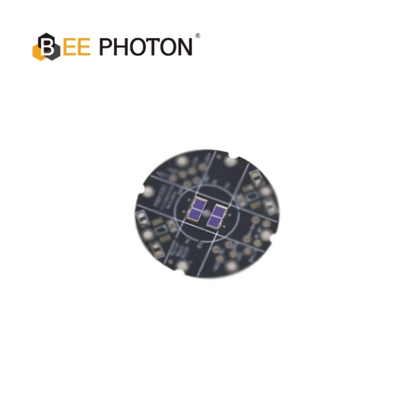
Fotodiodos PIN de Si para Galvo PDC-C2929
El PDC-C2929 es un chip de fotodiodo PIN de silicio de 920 nm económico. Este fotodiodo PIN de silicio de 920 nm ofrece un seguimiento estable y rentable de la posición del escáner.
Recommended Control Plan for Mass Production
A sensible control plan keeps retroalimentación de posicionamiento del escáner óptico under control at several stages rather than relying on one final test.
| Production stage | Control item | Reaction when out of control |
|---|---|---|
| Supplier release | Responsivity and segment matching | Hold shipment and review lot data |
| Incoming QA | Sample optical feedback test | Quarantine lot and verify test station |
| Die attach or assembly | Detector position and angle | Stop process and inspect placement system |
| Optical alignment | Total signal and center balance | Check beam geometry and fixture |
| PCB test | Gain, offset, and noise | Separate electronics failure from detector variation |
| Pre-calibration | Position slope and output range | Route abnormal units to diagnosis |
| Final calibration | Gain values and residual error | Trend by detector, emitter, and PCB lot |
| Reliability validation | Hot, cold, and ageing response | Review design margin and material changes |
Reaction rules should be written before a lot fails. Otherwise, every out-of-control result turns into a meeting about whether the chart “really matters.”
Questions to Ask a Photodiode Supplier
When discussing retroalimentación de posicionamiento del escáner óptico consistency with a supplier, ask direct questions:
- Are sensitivity limits controlled per unit, per wafer, or only through sample testing?
- Is segment matching measured on every die or on a sample basis?
- What wavelength, spot size, optical power, bias, and temperature are used?
- Can lot-level measurement data be provided?
- Are wafer lots kept separate during packing?
- What process changes trigger customer notification?
- Can tighter bins be supplied for sensitivity or segment balance?
- How are bare dies protected from contamination and mechanical damage?
- Can the supplier test using a customer-defined condition?
- What traceability remains after shipment?
Share your real optical conditions. Without them, the supplier may optimize a measurement that has weak correlation with your scanner.
For detector selection, lot-consistency discussions, or sample requirements, contact the BeePhoton technical sales team or send an email to info@photo-detector.com.
A Practical Action Plan
If your calibration line is already struggling with inconsistent retroalimentación de posicionamiento del escáner óptico, use this order:
- Freeze the test firmware and fixture configuration.
- Confirm source wavelength, optical power, and warm-up behavior.
- Run repeatability and reproducibility checks.
- Measure a stable golden sample.
- Separate results by detector lot, emitter lot, PCB lot, and station.
- Compare total responsivity, segment balance, center offset, and position slope.
- Perform component swap tests.
- Correlate incoming detector data with final calibration values.
- Set measurable supplier limits.
- Introduce binning or pre-calibration screening if needed.
- Monitor the process with control charts.
- Review the limits after enough stable production data exists.
This sequence avoids a common mistake: tightening the photodiode specification before proving which detector characteristic actually drives calibration time.
Make the Next Production Run Easier
Inconsistent scanner feedback does not usually disappear after one supplier complaint. It improves when the detector specification, optical test method, assembly controls, and calibration data all speak the same language.
If your QA team is seeing wider gain values, center-offset movement, repeated calibration, or unexplained scanner sensor batch consistency issues, start with the raw data. Then compare that data with the detector lot and actual optical conditions.
BeePhoton can discuss PDC-C2929 positioning chip selection, silicon PIN optical feedback requirements, segmented detector options, and lot-level evaluation needs. Bring the wavelength, spot size, circuit diagram, expected photocurrent range, and current calibration data. That makes the conversation much more useful.
Review available products on the BeePhoton photodetector website o request technical information and a quotation. A clear sensitivity and matching requirement now can save a lot of calibration work later. No one enjoys fixing the same batch problem twice.
Frequently Asked Questions About Optical Scanner Positioning Feedback
¿Cuál es la causa principal de la inconsistencia en la retroalimentación de posicionamiento del escáner óptico?
No existe una única causa universal. Entre los factores contribuyentes más comunes se encuentran la variación en la responsividad del fotodiodo, el desajuste de segmentos, los cambios en la longitud de onda del emisor, la deriva de la potencia óptica, los errores de posición del haz, la tolerancia de ganancia del amplificador y la repetibilidad del utillaje.
Comience midiendo una unidad patrón en la misma estación. A continuación, desglosen los datos de producción por lote de detector, lote de emisor, lote de PCB y utillaje. Si el cambio sigue al detector durante una prueba de intercambio, investigue la responsividad, el equilibrio de segmentos, la geometría o el ensamblaje del detector.
¿Puede la calibración del firmware eliminar por completo las diferencias de sensibilidad de los fotodiodos?
El firmware puede compensar las diferencias predecibles de ganancia y desviación dentro de un rango razonable. No puede corregir de manera confiable el desajuste severo de segmentos, el recorte del haz, la linealidad deficiente, el ruido excesivo, la contaminación óptica o un margen de señal inadecuado.
Los límites de corrección de firmware muy amplios también pueden ocultar un proceso de deriva en los componentes. Esto dificulta la resolución de problemas futuros y puede reducir el margen de rendimiento en temperaturas extremas.
¿Cómo debe medirse la consistencia de lote de los sensores del escáner?
Mida al menos la fotocorriente total, el equilibrio de segmentos, el desplazamiento del centro, la sensibilidad de posición, la linealidad y el ruido bajo condiciones ópticas y eléctricas controladas.
Utilice la misma longitud de onda, potencia óptica, tamaño del haz, posición del detector, polarización, ganancia, firmware y temperatura. Informe la media, la desviación estándar, el rango y la identidad del lote. Los gráficos de control son útiles una vez que el sistema de medición es estable.
¿Es mejor 920 nm o 940 nm para la retroalimentación óptica con PIN de silicio?
Ninguna longitud de onda es automáticamente mejor. La elección depende del emisor, la respuesta espectral del fotodiodo, los materiales ópticos, el rechazo de la luz ambiental, el margen de la señal y la disponibilidad de suministro.
Evalúe el par completo detector-emisor. Un diseño que utilice una fuente de 920 nm puede considerar el fotodiodo PIN de silicio PDC-C2929, mientras que un sistema centrado en 940 nm puede revisar la opción PDC-C2928-NIR-B. Confirme la compatibilidad real mediante pruebas.
¿Debería someterse a una prueba óptica cada fotodiodo de posicionamiento?
Eso depende del riesgo de la aplicación, la capacidad del proceso del proveedor, el coste de calibración y los requisitos de trazabilidad.
Para la producción de gran volumen, las pruebas 100% de unas pocas características rápidas pueden resultar más económicas que una caracterización óptica completa. Un enfoque común consiste en examinar la fotocorriente total y el equilibrio de segmentos en cada dispositivo, para luego realizar escaneos de posición detallados en las muestras. El plan adecuado debe basarse en el riesgo real de defectos y el coste de medición.
¿Cómo podemos reducir el tiempo de calibración sin rediseñar el escáner?
Agregue un paso de cribado previo a la calibración, controle los lotes de detectores, mida la salida del emisor, mejore la repetibilidad de los accesorios y agrupe los detectores por sensibilidad o equilibrio según sea apropiado.
También examine los valores de calibración almacenados por lote de componentes. Si un lote de detectores requiere de manera constante un rango de ganancia diferente, la clasificación por parte del proveedor o los ajustes iniciales específicos por lote pueden reducir el número de iteraciones de calibración.
¿Qué información debemos proporcionar al solicitar una cotización de fotodiodos?
Proporcione la longitud de onda objetivo, la potencia óptica, el tamaño del punto, el requisito de área activa, la configuración de segmentos, la fotocorriente esperada, la polarización inversa, el rango de temperatura, la cantidad anual, el formato de empaque y el requisito de consistencia de sensibilidad.
Para una revisión técnica más rápida, incluya su diseño óptico y el circuito de retroalimentación. Puede enviar estos detalles a través de Página de contacto de BeePhoton y solicitar muestras, información técnica o una cotización de producción.