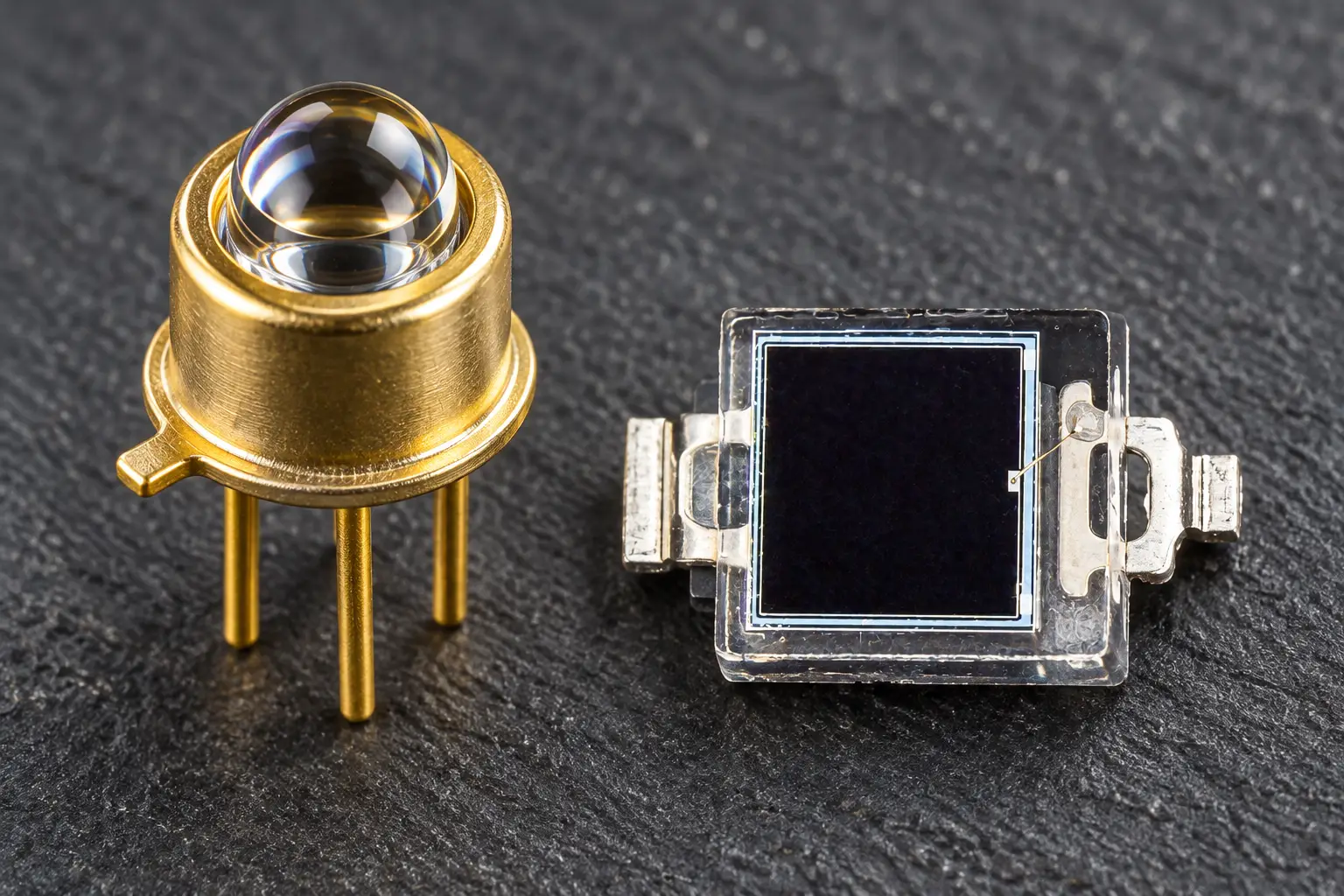
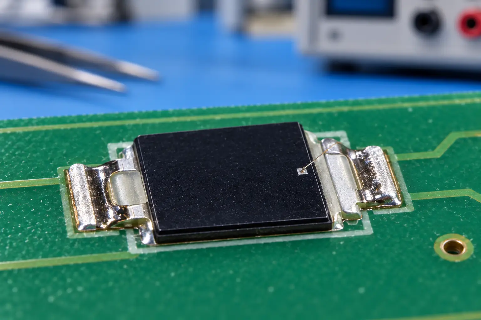
Every seasoned quality director has lived through some version of this nightmare: an industrial automation line or an outdoor solar monitoring installation starts glitching twelve months into field deployment. There is no fire, no dramatic bang. Instead, optical control loops gradually lose calibration, signal-to-noise ratios collapse, and microcontrollers throw intermittent fault codes.
When you drag those failed optical sub-assemblies back into the lab for root-cause failure analysis, the culprit is almost never the heavy-duty power stage or the primary processing unit. It is almost always a budget optical sensor whose package degraded under ambient field humidity.
Field Failure Reality Check: In non-hermetic optoelectronic packaging, over 70% of premature field failures trace back to interfacial moisture permeation, bond-wire fatigue, and uncalibrated dark current drift caused by sub-standard environmental qualification.
If you build optical equipment designed to run ten to fifteen years in real-world environments—think coastal factory floors, high-humidity textile plants, or unconditioned utility substations—specifying a fotodiodo dual 85 probado is not a luxury. It is the single most important line of defense between steady gross margins and catastrophic warranty recalls.
Here is the engineering reality behind Temperature-Humidity-Bias testing, thermal shock endurance, burn-in screening, and packaging tolerances for industrial optoelectronics.
The Physics of 85°C / 85% RH: What Actually Destroys a Standard Optical Sensor?
Most procurement teams look at a datasheet rating of -40°C to +85°C operating temperature and assume the component can handle humid heat. That assumption causes expensive mistakes. Operating in dry heat is straightforward; surviving steady-state moisture ingress under active electrical bias is brutally difficult.
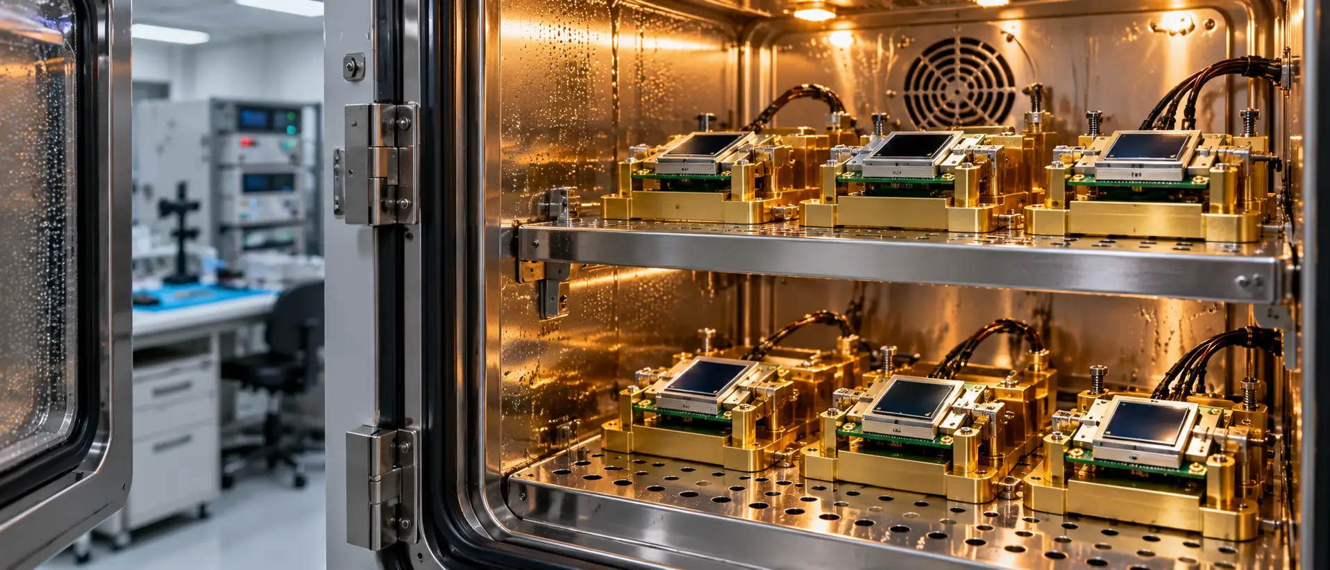
When an optical detector sits inside an environmental chamber at 85°C and 85% Relative Humidity under active reverse bias—often referred to as Temperature Humidity Bias (THB) testing governed by standards like JEDEC JESD22-A101—three distinct degradation mechanisms occur simultaneously:
Moisture and Bias Degradation Sequence:
- Continuous moisture ingress (85% RH) permeates the clear epoxy matrix.
- Delamination develops along the leadframe and silicon boundaries.
- Trace ionic contaminants (Cl-, Na+) dissociate under electric bias (-5V to -20V VR).
- Parasitic surface leakage channels form, driving dark current (Id) from picoamps to microamps.
- Galvanic corrosion attacks wire bond interfaces, leading to open-circuit field failure.
1. Polymer Permeation and Interfacial Delamination
Clear optical encapsulation epoxies and silicones are inherently hygroscopic. Water vapor molecules diffuse through the polymer matrix over time. Once moisture reaches the interface between the molding compound, the silicon die, and the metallic leadframe, adhesive bonds break down. This micro-delamination acts as an internal moisture reservoir, shifting the optical refractive index and generating internal reflections that degrade spectral responsivity. A genuine fotodiodo dual 85 probado uses specialized polymer formulations engineered to maintain adhesive bond strength even under extreme saturation.
2. Ionic Migration and Dark Current Explosion
Moisture alone does not kill silicon; ionic impurities carried by moisture do. Trace hydrolyzable chlorides, bromides, and sodium ions left behind from low-grade epoxy curing agents dissociate in the presence of water vapor. Under active reverse bias voltage, these ions migrate toward the p-n junction passivation perimeter.
The resulting surface inversion channels cause the dark current to skyrocket from picoamps (pA) to tens or hundreds of nanoamps (nA). For precision industrial instrumentation relying on linear photodiode response at low illumination, that dark current drift ruins dynamic range. Integrating a qualified fotodiodo dual 85 probado prevents this ionic migration through high-purity wafer passivation.
3. Anodic Galvanic Corrosion of Bond Pads
Where aluminum wire bonds meet gold bond pads, galvanic couples form. Trapped moisture combined with bias creates an active electrochemical cell. The aluminum dissolves, forming aluminum hydroxide while hydrogen gas evolves beneath the wire ball:
2Al + 6H2O -> 2Al(OH)3 + 3H2
This chemical reaction degrades mechanical pull strength, increases contact resistance, and eventually causes an open circuit. A verified fotodiodo dual 85 probado is built specifically with purified passivations, balanced epoxies, and corrosion-resistant metallization to withstand 1,000 continuous hours of this stress without package breakdown.
Calculating Lifetime: Applying Peck’s Acceleration Model
How does 1,000 hours of 85°C/85% RH testing translate to real-world performance? In reliability engineering, we do not guess; we use Peck’s empirical acceleration model for temperature-humidity-bias life testing, a cornerstone methodology documented by organizations like IEEE y NIST.
Peck’s relationship calculates the Acceleration Factor (AF) between accelerated test conditions and baseline field conditions:
AF = (RH_stress / RH_use)^n * exp((Ea / k) * (1 / T_use – 1 / T_stress))
Dónde:
- RH_stress: Relative humidity in test chamber (85% = 0.85)
- RH_use: Relative humidity in field environment (for example, 50% = 0.50)
- n: Humidity acceleration exponent (typically 2.7 to 3.0 for semiconductor packaging)
- Ea: Activation energy for moisture-induced degradation (typically 0.8 eV to 0.9 eV for silicon epoxy interfaces)
- k: Boltzmann’s constant (8.617 x 10^-5 eV/K)
- T_use: Absolute temperature of the field operating environment in Kelvin (for example, 30°C = 303.15 K)
- T_stress: Absolute temperature of the accelerated test chamber in Kelvin (85°C = 358.15 K)
Let us examine the real math for an industrial optical sensor operating in an ambient factory setting at 35°C (308.15 K) and 60% RH (0.60), assuming conservative parameters of n = 2.7 and Ea = 0.8 eV:
- Humidity Acceleration Component:
(0.85 / 0.60)^2.7 = (1.4167)^2.7 = 2.56 - Thermal Acceleration Component:
(Ea / k) = 0.8 / (8.617 x 10^-5) = 9284 K
(1 / 308.15 – 1 / 358.15) = (0.003245 – 0.002792) = 0.000453 K^-1
exp(9284 * 0.000453) = exp(4.205) = 67.06 - Total Acceleration Factor (AF):
AF = 2.56 * 67.06 = 171.7
Under these everyday conditions, 1,000 hours of validated reliability in a fotodiodo dual 85 probado chamber translates to:
1,000 hours * 171.7 = 171,700 hours = 19.5 years of continuous field life.
If your supplier only qualifies their optical sensors to 168 hours (standard commercial sampling), you are buying barely 3.2 years of guaranteed moisture resistance before uncalibrated dark current shifts begin corrupting your sensor readings. For infrastructure-grade hardware, choosing a fully certified fotodiodo dual 85 probado is the only way to avoid premature field failures.

Fotodiodo Si PIN Serie PDCP08 PDCP08-511
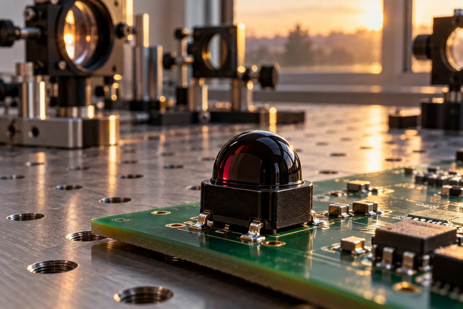
En PDCP08-511 es un sistema de alto rendimiento Fotodiodo PIN de epoxi negro diseñado para aplicaciones de infrarrojos de precisión. Envuelto en una resina epoxi negra especial, este sensor actúa eficazmente como un filtro de luz diurna, bloqueando las interferencias de la luz visible y maximizando la sensibilidad a 940 nm. Con una gran área activa de 2,9×2,9 mm y una baja corriente oscura, garantiza una detección fiable de señales para interruptores ópticos y sistemas de control remoto, incluso en entornos con luz ambiental ruidosa.
Thermal Fatigue: Why a 200 Thermal Cycle Sensor Outlasts the Rest
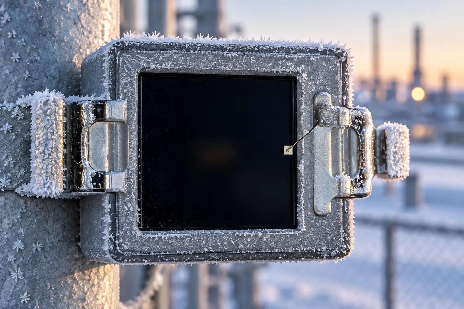
Moisture is only half the battle. Industrial machinery cycles on and off continuously, shifting through aggressive temperature swings. When a sensor transitions between sub-zero cold and elevated internal cabinet temperatures, Coefficient of Thermal Expansion (CTE) mismatch becomes destructive.
| Material Layer | Typical CTE (ppm/°C) | Mechanical Role in Photodiode | Thermal Vulnerability Under Cycling |
|---|---|---|---|
| Silicon Substrate | 2.6 | Active p-n junction die | Brittle fracture under localized bending |
| Copper Leadframe (C194) | 16.5 | Primary electrical/thermal base | Expands 6x faster than silicon die |
| Gold Bonding Wire | 14.2 | Anode and cathode interconnect | Heel fatigue at package bond points |
| Optical Clear Epoxy | 50.0 – 80.0 | Environmental seal & lens shaping | Expands up to 30x faster than silicon |
Because standard clear optical epoxy expands and contracts nearly thirty times faster than the underlying silicon die, severe shear stress concentrates directly on the die-attach fillet and wire bond necks during temperature shifts.
Thermal Cycle Failure Progression (-40°C to +105°C):
- At -40°C Low Soak: Clear epoxy shrinks aggressively, exerting intense downward compressive and inward lateral shear force on the gold wire bond neck.
- At +105°C High Soak: Epoxy expands rapidly, applying vertical tension that lifts the wire bond away from the silicon metallization pad.
- Accumulated Stress: Repeating this swing across 200 cycles induces low-cycle metal fatigue governed by the Coffin-Manson relationship, leading to heel micro-cracks and sudden open circuits.
Under standardized testing according to JEDEC JESD22-A104, devices transition from -40°C up to +105°C (or +125°C for harsher regimes) with a minimum 15-minute dwell time.
Commercial sensors often survive 50 to 100 cycles before microscopic cracks appear at the heel of the wire bond. Once micro-fractures initiate, intermittent high-resistance contacts occur, causing random signal dropout under mechanical vibration.
Un calificado 200 thermal cycle sensor relies on specialized stress-relieving packaging architectures:
- Optimized epoxy formulations that maintain an elastic plateau across wide operating temperatures.
- Automated wire loop profiles that preserve arch curvature, distributing strain evenly away from the fragile wire bond neck.
- Thermally matched silver-loaded die-attach adhesives that absorb lateral shear forces instead of transferring them into the silicon lattice.
Evaluating compliance against MIL-STD-883 Method 1010 ensures that a fotodiodo dual 85 probado survives aggressive thermal cycling without mechanical micro-cracking or bond delamination.
Weeding Out Infant Mortality: The 48h Burn-In Photodetector Regimen
Why do unvalidated optical sensors fail within the first few weeks of field deployment? The answer lies in the classic semiconductor reliability bathtub curve:
The Bathtub Curve Stages:
- Infant Mortality Period: High initial failure rate driven by latent manufacturing defects (passivation pinholes, crystal micro-fractures, sub-micron voids). A dedicated 48h fotodetector de quemado process catches and eliminates these defects at the factory.
- Useful Life Period: Low, constant, random failure rate where the fotodiodo dual 85 probado operates predictably for decades.
- Wear-Out Period: End-of-life failures caused by long-term chemical aging and packaging degradation, accurately predicted by Peck’s model.
Early failures are driven by latent micro-defects:
- Pinholes in the silicon nitride or silicon dioxide dielectric passivation layer.
- Microscopic silicon crystal dislocations introduced during high-speed wafer sawing.
- Sub-micron voids in the die-attach epoxy that create local hot spots under illumination or bias.
Without factory screening, these marginal devices ship out to your manufacturing line. They pass incoming inspection at ambient room temperature, get soldered into your sub-assembly, run for a few hundred hours in the field, and suddenly fail.
A rigorous 48h fotodetector de quemado protocol subjects every production batch to steady electrical and thermal acceleration:
- Continuous elevated reverse bias voltage (VR = 10V to 20V) applied across the junction.
- Chamber temperatures held steadily between 100°C and 125°C for 48 uninterrupted hours.
- Automated post-burn-in parameter screening for dark current drift and breakdown voltage stability.
If a photodiode possesses a latent defect in its passivation layer, the combination of electric field stress and thermal excitation accelerates defect propagation on our factory floor, long before it can reach your assembly lines.
Testing data proves that a standardized 48-hour burn-in eliminates over 95% of early semiconductor infant mortality, ensuring that your Bill of Materials contains only stable, mature devices. Specifying a fotodiodo dual 85 probado with burn-in screening safeguards your system against early life failures.
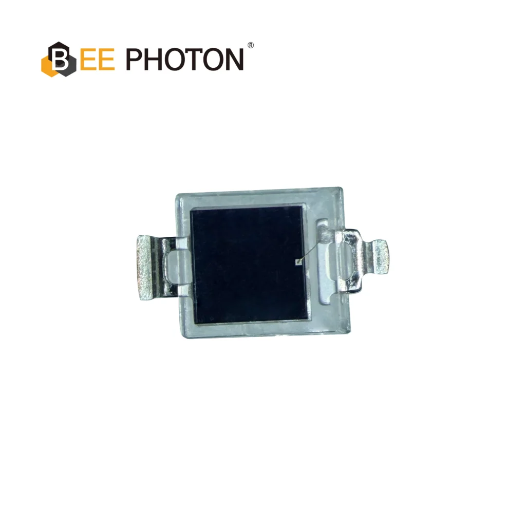
Fotodiodo Si PIN Serie PDCP08 PDCP08-501
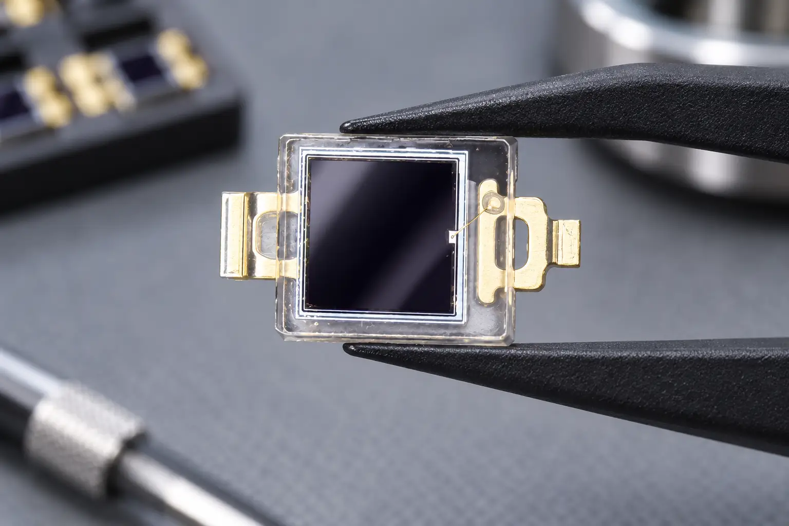
Detección de alto rendimiento: El PDCP08-501 es un fotodiodo PIN de silicio de alta velocidad con ventana transparente.
Especificaciones: Con un área activa de 2,9×2,9 mm, este fotodiodo PIN ofrece una baja corriente oscura y una alta capacidad de respuesta, lo que lo convierte en un sensor ideal para interruptores ópticos generales y sistemas de detección de luz.
Mechanical Exactness: Why 5µm Die Bonding Accuracy Dictates Optical Coupling
Reliability is not just chemistry and thermal endurance; it is also dimensional precision. When building optical sensing arrays, spectrometers, optical encoders, or fiber-coupled monitoring systems, your optical efficiency depends entirely on mechanical tolerances.
Optical Coupling Tolerance Comparison:
- Standard Commercial Sensor (+/- 30µm Die Shift): With an incident light beam of 0.8mm targeting a 1.0mm active area, a 30µm placement shift causes the beam to strike the edge perimeter, resulting in an 18% optical clipping loss and uncalibrated channel mismatch.
- BeePhoton Precision Sensor (+/- 5µm Die Shift): Centering accuracy keeps the incident beam locked in the center of the active area, holding coupling variance to under 0.2% across thousands of assembled boards.
A frequent failure mode in precision optical instruments is signal drift caused not by electrical failure, but by die placement shift during packaging. Standard commercial pick-and-place equipment holds die placement tolerances around +/- 30µm to +/- 50µm, with angular rotational errors of +/- 2° to +/- 3°.
When mounting a PIN photodiode behind a narrow optical slit, a focusing lens, or an aperture, that mechanical variance creates direct measurement error:
- Aperture Clipping Losses: If an incident optical beam measures 0.8 mm in diameter and hits an active area of 1.0 mm x 1.0 mm, a 30 µm placement shift brings the beam edge dangerously close to the active area boundary. Any thermal expansion or housing movement can clip the beam, generating false optical loss readings.
- Channel-to-Channel Crosstalk: In multi-channel optical sensing arrays, uneven die placement creates non-uniform cross-talk and phase offsets that calibration software cannot easily correct.
- Angular Tilt Distortion: Angular die tilt relative to the leadframe seating plane alters the incident angle of incoming light, changing surface reflectivity governed by Fresnel reflection formulas:
R = ((n1 * cos(theta_t) – n2 * cos(theta_i)) / (n1 * cos(theta_t) + n2 * cos(theta_i)))^2
A shift of even two degrees off-axis can skew reflection losses by several percent, throwing uncalibrated gain errors into optical power meters.
By securing a strict precisión de adhesión de die de 5µm, BeePhoton locks every silicon die dead-center on its mechanical optical datum. This eliminates channel matching errors, guarantees clean optical lens coupling, and saves OEM integration engineers from writing complex software calibration routines to correct for messy hardware assembly tolerances. Each precision fotodiodo dual 85 probado delivers both optical alignment precision and long-term environmental ruggedness.
Engineering Breakdown: Commercial vs. Dual 85 Tested Photodiode
To understand why consumer-grade optical sensors fail in demanding industrial environments, look at how materials and validation standards differ across manufacturing classes:
| Parámetro / Característica | Fotodiodo comercial estándar | Industrial Grade BeePhoton Dual 85 Tested Photodiode | Failure Mode Prevented |
|---|---|---|---|
| THB Endurance (85°C / 85% RH) | 168 hours (sample check) | 1,000 hours (100% batch qualification) | Dielectric breakdown, dark current drift, wire corrosion |
| Thermal Cycling Range | 50 to 100 cycles (-20°C to +70°C) | 200+ cycles (-40°C to +105°C / +125°C) | Wire bond heel fatigue, package delamination |
| Infant Mortality Screening | Batch sampling / ambient spot check | 48-Hour high-temp reverse-bias burn-in | Early-life factory line assembly drops, latent pinholes |
| Die Placement Tolerance | +/- 30µm to +/- 50µm (+/- 2.5° tilt) | <= +/- 5µm (<= +/- 0.5° tilt) | Optical misalignment, lens coupling loss, channel crosstalk |
| Encapsulation Polymer | Standard optical grade epoxy | Low-halogen, high-Tg optical compound | Hydrolysis, yellowing under UV/blue, ionic migration |
| Leadframe Plating | Flash gold or plain matte tin | Thick gold or precision Ag-plated alloy | Whisker growth, intermetallic purple plague, contact oxidation |
| Dark Current Stability | Can drift >10x within 12 months | Stable within datasheet limits over 15+ years | Dynamic range loss, calibration drift, false threshold trips |
Choosing a properly validated fotodiodo dual 85 probado is not an added cost; it is an insurance policy against field repairs, shipping recalls, and lost OEM reputation.
Field Autopsy: The Real Cost of a $0.40 Component Shortcut
A few years ago, a prominent European manufacturer of commercial solar power inverters redesigned their maximum power point tracking (MPPT) array. To save costs, their procurement team replaced an industrial-grade optical sensor with an unvalidated commercial photodiode sourced from a low-tier broker. On paper, both parts shared the same peak wavelength, active area, and basic responsivity.
Within fourteen months of commissioning in a high-humidity environment in Southeast Asia, inverters began showing intermittent ground-fault isolation warnings. Maintenance crews visited installations repeatedly, finding that the internal optical arc-fault detection boards were reporting phantom arcing events.
| Financial & Operational Metric | The $0.40 Component Shortcut | The Qualified Dual 85 Tested Photodiode Alternative |
|---|---|---|
| Upfront BOM Savings | Saved $10,000 on 25,000 units ($0.40/unit) | Baseline component investment |
| 14-Month Field Failures | 420 inverter shutdowns in humid climates | 0 environmental false triggers |
| Warranty & Dispatch Costs | ~$380,000 in technician swaps and penalties | $0 in environmental warranty claims |
| Net Financial Outcome | -3,800% ROI on component savings | Protected margins and brand trust |
When our engineering team at BeePhoton assisted with the failure analysis, we decapsulated the failed sensors under an acoustic micro-imaging microscope. The findings were clear:
- High moisture permeation had dissolved chlorine traces from the cheaper epoxy, concentrating them around the anode wire bond.
- The photodiode dark current, originally specified at 0.5 nA, had drifted up to 180 nA under field heat and ambient humidity.
- The onboard amplifier circuit interpreted this leakage current increase as background optical emission from an electrical arc, triggering emergency plant shutdowns.
Replacing that unvalidated component with a certified fotodiodo dual 85 probado completely eliminated the issue. But the manufacturer had already absorbed over $380,000 in warranty claims, emergency field technician dispatches, and brand damage. Skimping on foundational optical testing to save pennies is one of the most dangerous gambles in industrial hardware engineering.
Application Matching: Choosing the Right Industrial Optical Sensor
Seleccionar un industrial grade optical sensor means pairing proven mechanical and environmental reliability with your specific optical bandwidth and optical system design. Here is how three of BeePhoton’s core PIN photodiodes solve industrial OEM challenges:
1. High-Noise Ambient Environments: Silicon PIN Photodiode PDCP08-511
When building optical edge switches, sorting barriers, or infrared communication modules that operate under bright ambient factory lighting or direct sunlight, ambient visible light can easily saturate your detector.
En fotodiodo PIN de silicio PDCP08-511 is molded in an advanced optical-grade black epoxy that acts as a physical daylight-blocking filter:
- Blocks ambient visible wavelengths (400 nm to 700 nm).
- Delivers maximum responsivity across the near-infrared spectrum (800 nm to 1100 nm).
- Fully qualified under fotodiodo dual 85 probado conditions, preventing epoxy hazing or optical transmittance loss even in humid, sun-drenched industrial environments.
2. High-Density Spatial Arrays: Silicon PIN Photodiode PDCP08-502
Space constraints often complicate optical sensing designs. In multi-channel laser diode power feedback loops, medical diagnostics, or tight instrumentation enclosures, footprint is critical.
En Si PIN photodiode PDCP08-502 delivers industrial-grade performance in a compact 2.9 mm x 2.8 mm footprint:
- Low profile, surface-mount design engineered with tight internal thermal management.
- Precision leadframe stamping designed to handle rapid solder reflow profiles without mechanical stress.
- Designed as a robust 200 thermal cycle sensor, delivering consistent junction stability for modular optical instruments.
- Fully screened as a fotodiodo dual 85 probado to guarantee package stability in high-density board designs.
3. Broad-Spectrum Precision Monitoring: Silicon PIN Photodiode PDCP08-501
For analytical instrumentation, process-line spectrophotometers, and laboratory optical power measurement systems, flat responsivity and rock-bottom dark current are non-negotiable.
En Si PIN photodiode PDCP08-501 offers versatile optical sensing performance:
- Broad spectral sensitivity covering the entire visible-to-NIR spectrum (400 nm to 1100 nm).
- Ultra-low baseline dark current (pA level) and fast rise/fall times for high-speed pulse detection.
- Screened through a full 48h fotodetector de quemado protocol to eliminate infant mortality and guarantee measurement stability from day one.
- Certified as a fotodiodo dual 85 probado to ensure decade-long linear performance in precision laboratory instruments.

Fotodiodo Si PIN Serie PDCP08 PDCP08-502
El PDCP08-502 es un fotodiodo PIN de silicio de 2,9×2,8 mm de alta respuesta diseñado para aplicaciones fotoeléctricas de precisión. Con baja capacitancia de unión, baja corriente oscura y un amplio rango espectral (340-1100 nm), es el componente ideal para interruptores ópticos y módulos de detección compactos que requieren una salida de señal estable y rápida.
Preguntas más frecuentes (FAQ)
¿Qué hace que un fotodiodo dual 85 probado sea diferente de un fotodiodo comercial estándar?
A fotodiodo dual 85 probado se somete a validación a 85°C y 85% de humedad relativa bajo sesgo inverso durante 1.000 horas, siguiendo normas como JEDEC JESD22-A101. Los fotodiodos comerciales estándar suelen someterse a pruebas solo de 96 a 168 horas, o se califican exclusivamente mediante modelado matemático sin verificación en cámara climática. Los componentes de grado industrial cuentan con epóxicos especializados de bajo contenido de cloro, interfaces de unión del chip de alta adhesión y capas de pasivación resistentes a la corrosión, diseñados específicamente para eliminar la deriva de la corriente oscura inducida por la humedad.
¿Cómo reduce las pruebas de burn-in de 48 horas los costos globales de producción del sistema?
Los defectos latentes de semiconductores, como las microfisuras en obleas submicrónicas, los pinholes de pasivación y los bucles frágiles de enlace de alambre, a menudo superan las pruebas funcionales básicas posteriores al embalaje. Estos componentes marginales fallan principalmente durante sus primeras 24 a 72 horas de operación real. Mediante el uso de un 48h fotodetector de quemado, los OEMs rechazan las fallas de mortalidad infantil dentro de la fábrica de componentes en lugar de hacerlo durante las pruebas de calidad finales del producto o, peor aún, después del despliegue en el sitio del cliente. Elegir un fotodiodo dual 85 probado con burn-in integrado reduce las tasas de desecho de ensamblaje y reduce significativamente la exposición a garantías en campo.
¿Por qué importa la precisión del bonding de die de 5µm si nuestra abertura óptica es grande?
Si bien una apertura más grande puede capturar físicamente la luz de un die mal centrado, el desplazamiento de alineación dimensional altera su geometría de captura óptica. Un die colocado fuera de centro o inclinado varios grados cambia el ángulo efectivo de incidencia, introduciendo sensibilidad a la polarización no deseada y alterando las pérdidas de reflexión óptica. Además, para el ensamblaje óptico automatizado, trabajar con una precisión de adhesión de die de 5µm en sus fotodiodo dual 85 probado componentes garantiza bancos de trabajo mecánicos confiables a lo largo de los lotes de producción. Esto elimina la necesidad de calibración manual, acelera el ensamblaje de placas y asegura un rendimiento óptico uniforme.
¿Puede un fotodiodo dual 85 probado manejar aplicaciones automotrices de alta vibración o robótica de fábrica?
Yes. Meeting dual 85 reliability requirements requires mechanical and interfacial integrity. Combining THB resistance with a 200 thermal cycle sensor rating ensures that bond wires, die attachment adhesives, and packaging compounds do not delaminate or work-harden under ongoing mechanical stress and thermal fatigue. This makes each fotodiodo dual 85 probado well-suited for industrial robotics, automotive under-the-hood monitoring, and high-vibration manufacturing equipment.
Engineering Dependability: Take the Next Step with BeePhoton
If you are designing next-generation optical hardware, your choice of photodetector directly determines your product’s field reliability. Do not let unvalidated commercial sensors jeopardize your industrial designs.
En BeePhoton, we design, package, and screen every fotodiodo dual 85 probado to the industry’s most rigorous benchmarks:
- 1,000-Hour Steady-State THB Qualification (85°C / 85% RH) to secure decade-long operational life in humid environments.
- 200+ Temperature Shock Cycles (-40°C to +105°C / +125°C) to eliminate thermal fatigue and wire bond fractures.
- 100% 48-Hour High-Temperature Burn-In Screening to eradicate infant mortality before shipment.
- Industry-Leading <= +/- 5µm Die Placement Precision for dependable optical alignment.
Protect Your Bill of Materials Today
Review our comprehensive catalog of industrial grade optical sensors or get in touch with our applications engineering team directly to request qualification reports, discuss custom optical packaging geometries, or order evaluation engineering samples for your next prototype build.
- Technical Inquiries & Volume Quotes: Contact BeePhoton Application Engineers
- Direct Engineering Support Email: info@photo-detector.com
- Primary Website: BeePhoton Industrial Optoelectronics