There is nothing—and I mean absolutely nothing—worse than shipping a batch of ICs, thinking you nailed the production run, only to have the client come back screaming about dead chips a week later.
You open the RMA report. The electrical test passed at wafer sort. The final test passed. But somewhere in the packaging process, a wire bond snapped, or a solder ball decided to create a void the size of a crater. And because it was encapsulated in black epoxy, nobody saw it.
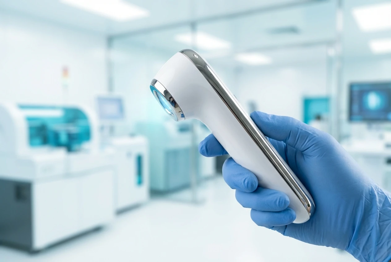
If you are running quality control in a packaging plant, you know this pain. Visible light inspection is useless once the lid is on. This is where X-ray inspection for electronics stops being a “nice-to-have” and becomes the only thing saving your reputation.
I’ve spent years messing around with different sensing tech, and I want to walk you through exactly how X-ray detectors for chip packaging work, not from a textbook perspective, but from the messy, practical reality of the factory floor. We’ll look at the math, the hardware, and why some detectors give you crisp images while others look like a blurry ultrasound from the 1980s.
Why Your Standard Inspection is Failing You
We used to rely heavily on acoustic microscopy (SAM) for delamination, and it’s great for that. But acoustic waves hate air gaps. If you need to see complex interconnects, flip-chip bumps, or Through-Silicon Vias (TSVs), you need photons with high energy.
The problem isn’t usually generating the X-rays; it’s detecting them efficiently.
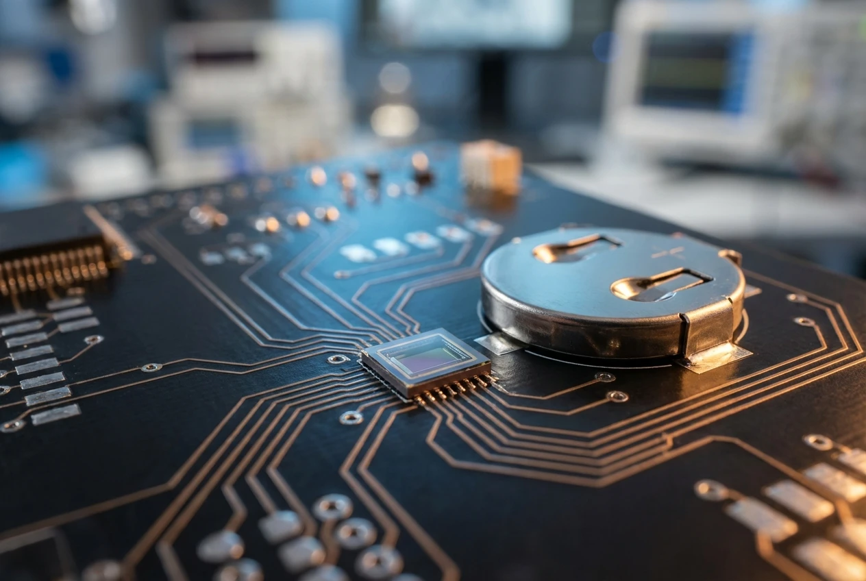
In semiconductor NDT (Non-Destructive Testing), we are dealing with micron-level features. A standard medical X-ray panel isn’t going to cut it. You need dynamic range. You need to distinguish between the silicon die, the copper leadframe, and the gold or copper bond wires.
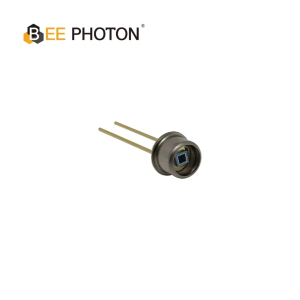
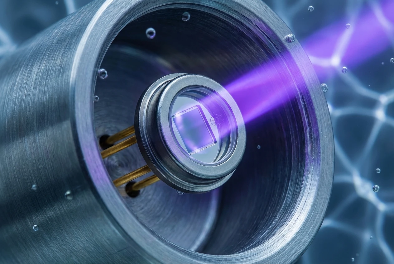
Si PIN Photodiode with UV sensitivity enchanced (190-1100nm) PDCT01-F01
Experience precise UV detection with our Quartz Window Si PIN Photodiode. Ideal for spectroscopy, it offers high sensitivity and low noise across 190-1100nm. This reliable Si PIN photodiode ensures accurate analytical results.
The Physics: How We actually “See” Through Silicon
Okay, I promised no heavy jargon, but we have to touch on the physics just a bit so you understand why buying cheap detectors is a waste of money.
When you fire X-rays at a chip package, the intensity drops as it passes through material. This is basic attenuation. The formula that rules our lives is:
I = I0 * e^(-mu * x)
Where:
- I is the intensity hitting the detector (what we see).
- I0 is the initial intensity from the source.
- e is Euler’s number (approx 2.718).
- mu is the linear attenuation coefficient (this depends on the material’s density and atomic number).
- x is the thickness of the material.
Here is the kicker: mu changes drastically based on what you are looking at.
Gold (Au) has a massive attenuation coefficient compared to Silicon (Si) or the epoxy mold compound. This is why gold wires show up as stark black lines on a white background (or white on black, depending on your software).
The Challenge:
Modern packaging is moving to Copper (Cu) wire bonding. Copper’s density is much closer to Silicon and the leadframe than Gold is. The contrast drops. If your detector has high noise (a low Signal-to-Noise Ratio), that copper wire blends right into the background. You won’t see the “wire sweep” (where the wire bends and shorts) until the chip burns out in the field.
Choosing the Right Detector: Scintillators vs. Direct Conversion
This is where I see people mess up the most. They look at a spec sheet, see “resolution,” and buy the cheapest option.
There are essentially two ways to catch those X-ray photons.
1. Indirect Detection (Scintillators)
This is the old school method. You have a material (like Cesium Iodide) that glows when X-rays hit it. It turns X-rays into visible light. Then, a photodiode array sits behind it to catch that light.
- Pros: Cheaper, robust.
- Cons: Light scatters. That “glow” spreads out, making the image slightly blurry. It reduces your MTF (Modulation Transfer Function)—basically, your sharpness.
2. Direct Detection (What you probably need)
This uses a semiconductor material that converts X-ray photons directly into electron-hole pairs. No light, no scattering.
If you are looking for sub-micron cracks in a solder bump, you want direct detection or high-end indirect systems coupled with quality photodiodes. Specifically, Si PIN photodiodes are the workhorses here. They offer incredibly low dark current, meaning when there is no X-ray, the signal is basically zero. This gives you that high contrast needed to see a copper wire against a copper leadframe.
At BeePhoton, we’ve seen clients switch from generic CMOS sensors to optimized Si PIN arrays and suddenly, they can see voids in BGA balls that were invisible before.
Common Defects You Can Finally Spot
When you have a solid chip packaging testing rig set up, here is what you are hunting for.
The “Head-in-Pillow” (HiP) Defect
This is a nasty one. It happens in Ball Grid Arrays (BGAs). The solder ball melts, but it doesn’t actually wet to the pad. It looks like a head resting on a pillow. Electrically, it might pass a quick test, but thermal cycling will break it.
A good X-ray detector shows the slightly different shape of the ball interface.
Wire Sweep
During the molding process, the liquid epoxy flows over the chip. If it flows too fast (or the wires are too thin), it pushes the wires like seaweed in a current. If two wires touch? Short circuit.
You need a detector with high spatial resolution to measure the curvature of the sweep.
Die Attach Voids
You glue the chip to the frame. If bubbles form in that glue (die attach paste), heat can’t escape. The chip overheats.
We calculate the “void percentage.”
Void % = (Area of Voids / Total Die Area) * 100
If your detector is noisy, it interprets noise as small voids, or misses real voids.

Si PIN Photodiode with UV sensitivity enchanced (320-1060nm) PDCC100-701
Our High Responsivity Si PIN Photodiode offers a superior signal for demanding applications. It excels in low-light UV detection from 320-1060nm.
Comparison: What Detector Fits Your Fab?
I threw together this table to help you compare. Don’t take it as gospel, but it’s a good rule of thumb.
| Feature | Si PIN Photodiodes | Standard CMOS Flat Panel | Image Intensifiers |
|---|---|---|---|
| Cost | Moderate | High | Low |
| Resolution | Very High | High | Low to Medium |
| Contrast | Excellent | Good | Poor |
| Durability | High (Radiation Hard) | Medium | Medium |
| Best For | Precision Wire Bond, Flip Chip | Large PCB Assemblies | Basic Casting inspection |
A Real World Scenario (Names Changed, Obviously)
Let me tell you about a case that kept me up at night.
We were working with a mid-sized OSAT (Outsourced Semiconductor Assembly and Test) company in Malaysia. Let’s call them “Fab X.” They were packaging power management ICs for automotive use.
The Problem:
They had a 0.5% field failure rate. In automotive, that is catastrophic. The chips were blowing up. They suspected the wire bonds were lifting off the pads (bond lift).
They were using an old Image Intensifier X-ray system. When they looked at the chips, everything looked gray. They literally couldn’t tell if the bond was attached or hovering 5 microns above the pad.
The Fix:
We swapped out the sensing element. We integrated a customized BeePhoton detector array using high-resistivity silicon.
The Result:
The contrast improved by roughly 400%. Suddenly, they could see the “crescent bond” shape clearly. It turned out, the bond wasn’t lifting—it was cracking at the heel due to incorrect ultrasonic power settings on the bonder.
They adjusted the bonder. Failure rate dropped to near zero.
They didn’t need a new X-ray source; they just needed better eyes.
Setting Up Your X-ray Station: Practical Tips
If you are buying or upgrading, keep these points in mind.
- Tube Voltage (kV) Matters:
Don’t just crank it to max power.- For plastic packages: 40-90 kV is usually the sweet spot.
- For ceramic or metal lids: You might need 120 kV+.
- Pro tip: Lower voltage often gives better contrast for low-density materials (like the epoxy), provided the X-rays can penetrate.
- Geometric Magnification:
You want the sample close to the source and the detector far away to zoom in.
Magnification (M) = Source-to-Detector Distance (SDD) / Source-to-Object Distance (SOD)
If your detector is bulky, you can’t get it close enough for high mag in some setups. Compact detectors win here. - Averaging Frames:
X-ray is a random process (quantum noise). To get a clean image, you grab 16 or 32 frames and average them.
SNR_new = SNR_single * sqrt(N)
Where N is the number of frames.
So, averaging 4 frames doubles your signal-to-noise ratio. Don’t be lazy—set the software to average.

Si PIN Photodiode with low dark current (350-1060nm) PDCC100-001
Looking for a custom Si PIN photodiode? Bee Photon provides OEM solutions with low dark current and a 350-1060nm range. We partner with B2B clients to develop photodiodes tailored to your specific needs.
FAQ: Questions Clients Always Ask Me
Q1: Can X-ray inspection damage the semiconductor chips?
Answer: generally, no. However, memory chips (Flash, DRAM) are sensitive to ionizing radiation. The “threshold voltage” of the transistors can shift if you blast them for too long. For standard logic or power chips, the dose during inspection is negligible. If you are inspecting EPROMs, check the datasheets for max rad dose.
Q2: Why is my X-ray image of the BGA ball oval instead of round?
Answer: This is usually a geometric distortion or the chip is tilted. If the detector isn’t perfectly perpendicular to the source, you get “keystone” effects. Or, you might actually have a squashed solder ball! Rotate the sample 90 degrees. If the oval rotates, it’s the ball. If the oval stays oriented the same way on screen, it’s your alignment.
Q3: How often do I need to calibrate the detector?
Answer: You should run a “gain and offset” correction (flat field correction) every time you start a shift or if the temperature changes significantly. Detectors have background noise patterns that shift with heat. It takes 2 minutes and makes your image 10x better.
Future-Proofing Your Inspection
The industry is getting weirder. We are stacking chips vertically (3D-IC). We are putting logic and memory side-by-side (Chiplets).
Standard 2D X-ray is struggling with this because the layers overlap. You look through the top chip and see the bottom chip’s wires confusing the image.
The industry is moving toward CT (Computed Tomography), where you rotate the sample and build a 3D model.
But guess what? CT requires hundreds of images taken very quickly. If your detector has “lag” (ghosting from the previous frame), your 3D reconstruction will look like garbage. Fast readout speed in detectors, like the ones found in modern Si PIN photodiodes, is critical for CT.
Why BeePhoton?
Look, I’m not here to give you a hard sell, but I am proud of what we build. At BeePhoton, we don’t just ship a box and wish you luck. We understand the specific energy ranges used in semiconductor NDT.
We know that a detector optimized for dental imaging is terrible for chip packaging. We tweak the scintillator thickness and the diode characteristics to match the low-contrast needs of electronics inspection.
If you are tired of squinting at grainy gray blobs and guessing if your wire bonds are intact, it’s time to upgrade your eyes.
Ready to see what you’ve been missing?
Don’t let a $2 chip ruin a $50,000 system.
- Reach out to us: Drop an email to info@photo-detector.com.
- Check the specs: Visit our site at https://photo-detector.com/.
- Get a quote: We can discuss your specific packaging type (QFN, BGA, CSP) and find the sensor that fits.
Visit our Contact Page today. Let’s make sure your chips leave the factory perfect, every single time.