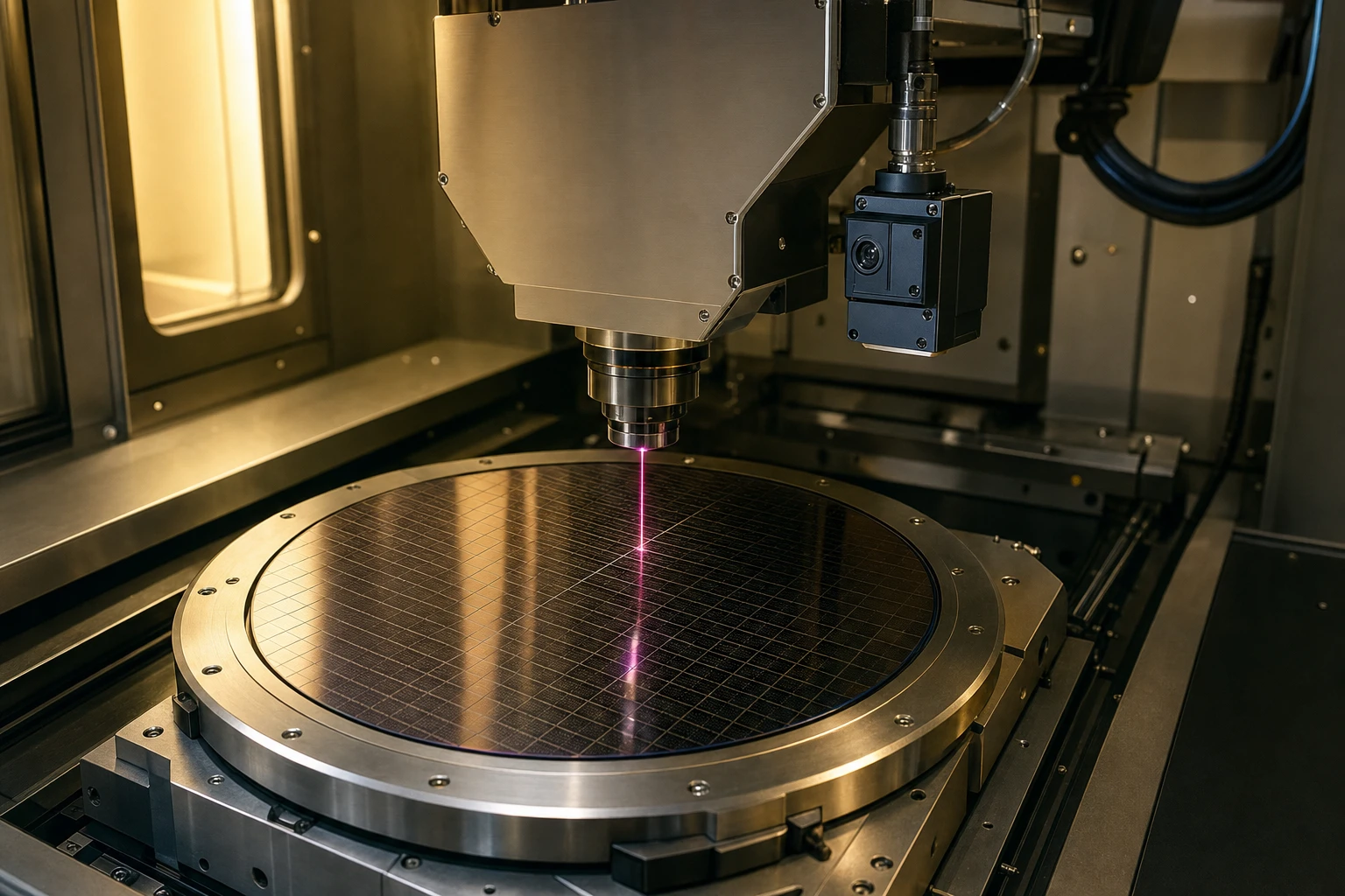
If you’re a designer working on optical systems and struggling to get enough signal strength at the receiving end without cranking up the light source power, you’re not alone. Boosting photosensitivity A/W (also called responsivity) in silicon photodiodes can make a real difference. Over the years tinkering with Si PIN photodiodes, I’ve seen how small tweaks in design and setup push that A/W number higher, giving you cleaner, stronger signals without burning more energy on the transmit side.
Photosensitivity A/W tells you how much photocurrent you get per watt of incident light. Higher values mean your detector turns weak light into usable electrical signals more efficiently. For silicon-based devices like Si PIN photodiodes, typical peak responsivity sits around 0.5 to 0.7 A/W in the visible to near-IR range, depending on wavelength and construction. At longer wavelengths like 1064 nm, it often drops to 0.4-0.45 A/W without optimizations.
In this article, we’ll walk through practical ways to maximize photosensitivity A/W in silicon photodiodes. I’ll share what actually works based on real device behavior, some formulas you can use right away (converted to plain text for easy reading), and tips tailored for system designers who need better Si PIN efficiency without major overhauls.
Why Photosensitivity A/W Matters for Your Designs
Think about it: your laser or LED is already pushing as much power as thermally safe or power-budget allows. The bottleneck often sits at the detector. Improving responsivity directly increases signal current, which improves signal-to-noise ratio (SNR) and lets you maintain performance at lower input powers.
Responsivity R in A/W connects to quantum efficiency η by this relation:
R (A/W) = η × (λ in µm) / 1.24
Where λ is the wavelength. For example, at 800 nm (0.8 µm) with 90% quantum efficiency, you get roughly 0.58 A/W. This isn’t theory — it’s what you’ll see on datasheets from good manufacturers.
Si PIN photodiodes shine here because the intrinsic layer allows better charge collection and lower capacitance compared to simple PN diodes. But raw material properties set limits. Silicon’s absorption coefficient drops sharply beyond 900 nm, so light passes through without generating many electron-hole pairs unless you engineer the structure smartly.
Understanding Responsivity and Quantum Efficiency in Si PIN Photodiodes
Responsivity isn’t constant. It varies with wavelength, bias voltage, temperature, and device thickness. Peak response for standard silicon photodiodes often lands between 800-950 nm.
Quantum efficiency (QE) is the percentage of photons that produce collected charge carriers. External QE accounts for reflection and other losses. To push photosensitivity A/W, you chase higher QE while matching the wavelength.
Common formula for ideal responsivity (at 100% QE):
R = (λ × q) / (h × c)
But in plain numbers, the simplified version R ≈ η × λ(µm) / 1.24 works well for quick calculations.
I’ve tested devices where applying moderate reverse bias (5-20V depending on the diode) slightly boosts responsivity by improving charge collection in the depletion region. The gain isn’t huge — maybe 5-10% — but every bit helps when you’re fighting for signal.
Temperature also plays a role. Responsivity can shift because the silicon bandgap narrows with heat, extending the long-wavelength response a little but sometimes increasing dark current, which hurts noise performance.
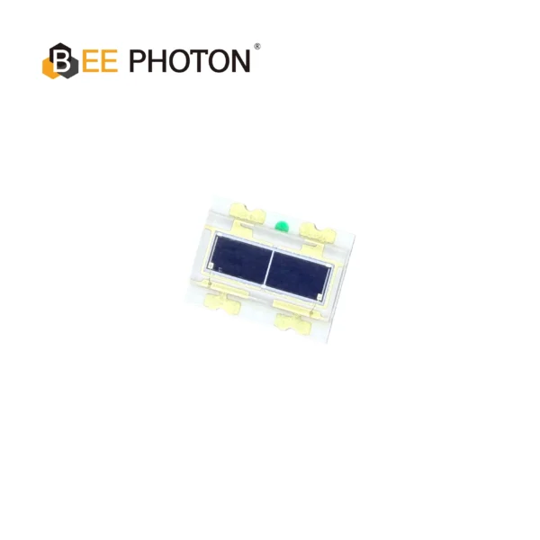
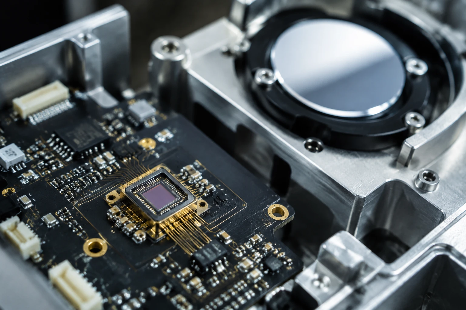
Si PIN Photodiode Array PDCA02-602
The Bee Photon PDCA Series is engineered specifically as a Background Suppression Photodiode to solve complex detection challenges in industrial environments. By utilizing a high-precision two-segment architecture (PD A and PD B), this device allows for differential signal processing, effectively filtering out background interference. It is the premier choice for manufacturers designing reliable background suppression optical switches and proximity sensors.
Key Factors That Limit or Boost Photosensitivity A/W
From hands-on work with various Si PIN photodiodes, here are the big levers:
- Active Layer Thickness and Absorption: Silicon needs enough thickness to absorb light, especially at NIR wavelengths. Too thin and photons slip through; too thick and you risk higher capacitance or slower speed. For 1064 nm, simulations and real parts show 200-400 µm thickness often hits sweet spots when combined with back reflectors.
- Surface Reflection and Anti-Reflection Coatings: Plain silicon reflects 30%+ of light at some wavelengths. Good AR coatings can cut that loss dramatically, directly lifting external QE and thus photosensitivity A/W.
- Light Trapping Techniques: Adding diffuse or specular reflectors on the rear side lets unabsorbed light bounce back for a second (or third) pass. One study found responsivity climbing from ~0.4 A/W to 0.58 A/W at 1064 nm with proper rear diffuse reflectors on thicker devices.
- Depletion Region Optimization: In PIN structures, widening the i-layer under bias improves collection efficiency and reduces recombination losses.
- Material Quality and Surface Passivation: Lower defect densities mean fewer recombination centers. Good passivation cuts surface recombination, especially important for blue/UV response but helpful across the board.
Here’s a quick comparison table of typical responsivity ranges for silicon photodiodes:
| Wavelength Range | Typical Responsivity (A/W) | Common Limitations | Optimization Tips |
|---|---|---|---|
| 400-700 nm (Visible) | 0.4 – 0.6 | Surface recombination | Blue-enhanced designs, thin front layers |
| 800-950 nm (NIR peak) | 0.5 – 0.7 | Moderate absorption | Standard AR coatings |
| 1064 nm (YAG) | 0.38 – 0.58 | Weak absorption | Light trapping, thicker i-layer, reflectors |
| >1100 nm | Drops sharply | Bandgap cutoff (~1100 nm) | Not suitable for standard Si |
Data drawn from manufacturer characteristics and technical literature. Real values vary by specific model — always check the datasheet for your candidate part.
Practical Ways to Maximize Responsivity in Silicon Photodiodes
Let’s get into the actionable stuff. These aren’t exotic lab tricks — they’re things you can specify when selecting or integrating Si PIN photodiodes.
Choose or Specify the Right Device Structure
Go for PIN over basic PN when speed and sensitivity both matter. The intrinsic region lets you apply bias to sweep carriers efficiently without high dark current.
For NIR work, look for “IR-enhanced” or “YAG-optimized” Si PIN photodiodes. Some makers tweak doping and add gettering to improve long-wavelength response.
In one project I worked on, switching to a thicker i-layer device with rear reflector bumped effective photosensitivity A/W enough to meet SNR targets without increasing laser power. The system designer was happy because it kept power budgets and thermal loads in check.
Apply Proper Bias and Operating Conditions
Don’t run at zero bias if you can avoid it. Moderate reverse bias widens the depletion zone, improving collection and slightly raising responsivity. But watch capacitance — it drops with bias, which is usually good for bandwidth.
Temperature control helps too. If your application runs hot, account for the slight responsivity shift and increased noise.
Optical Interface Optimization
- Use AR-coated windows or direct coupling with index-matching materials.
- Align the beam to the active area center for best uniformity. Good devices show <2% nonuniformity over 80% of the active area.
- Consider microlenses or concentrators if your spot size is small.
Light Trapping for Higher Si PIN Efficiency at Problem Wavelengths
At 1064 nm, silicon’s absorption length is long. Without help, much light transmits through. Rear-side diffuse reflectors scatter light, increasing path length inside the silicon. Studies show this can push responsivity toward 0.58 A/W or better on optimized geometries (around 200-300 µm thick, moderate area 0.6-2.5 mm² to balance capacitance and dark current).
Specifying custom or semi-custom parts with these features can pay off in high-volume or high-performance designs.
Comparing Standard vs. Optimized Si PIN Photodiodes
Standard off-the-shelf silicon photodiodes give decent performance, but optimized ones for specific wavelengths deliver more.
For example, at 930 nm some parts reach ~0.58 A/W. At 1064 nm, standard might give 0.4 A/W while light-trapping versions approach 0.55+ A/W. The difference translates directly to stronger received signals or relaxed requirements on the transmitter.
When selecting from categories like Si PIN photodiodes, look beyond headline responsivity — check the full spectral curve, capacitance at your operating bias, and dark current specs. They all interact with your overall system SNR.
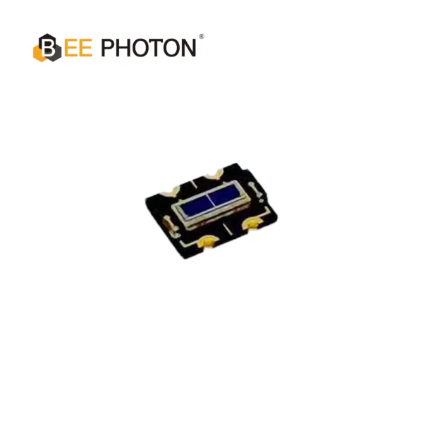
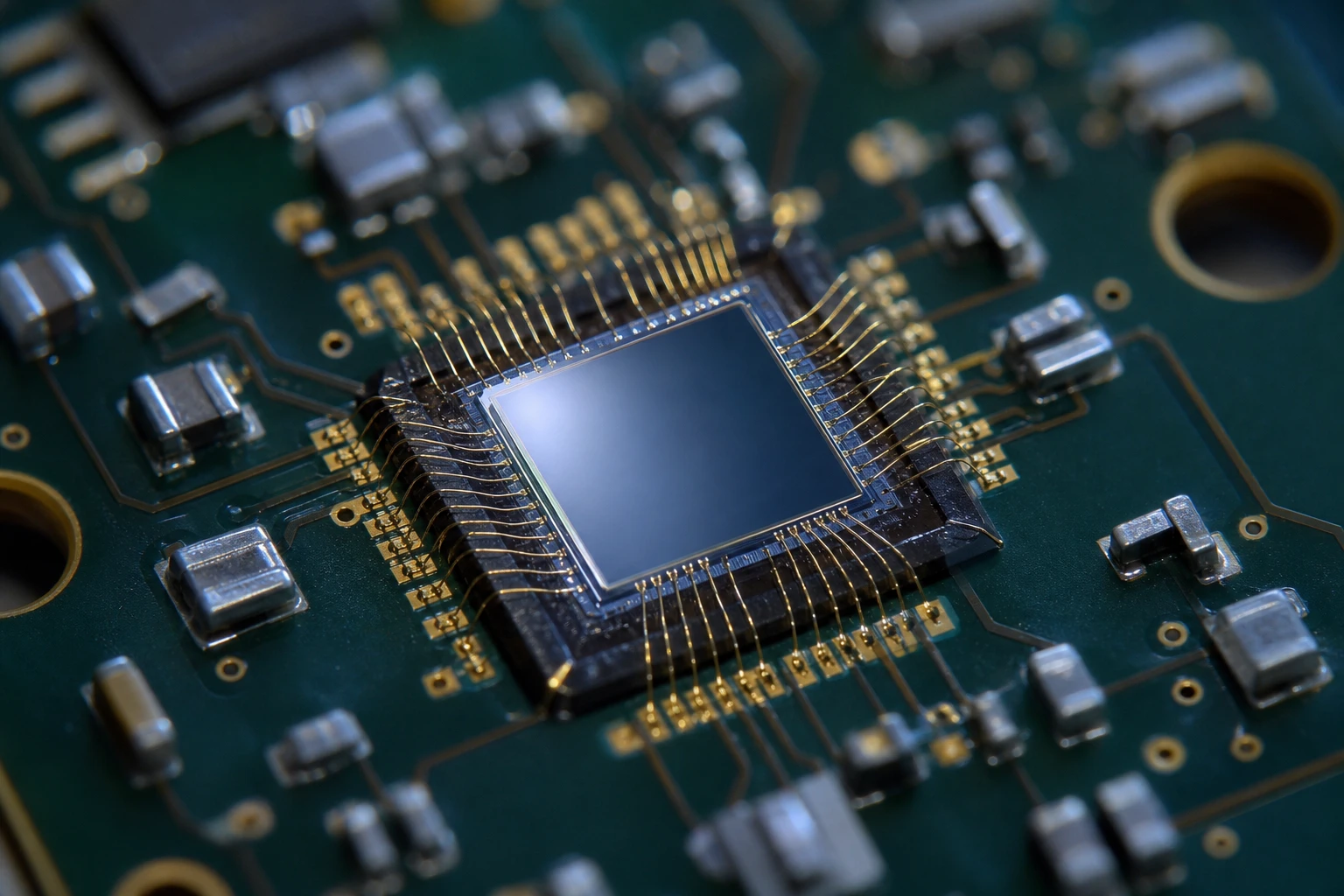
Si PIN Photodiode Array PDCA02-601
The Bee Photon PDCA Series is a precision-engineered Dual PIN Photodiode designed for high-end industrial sensing. Unlike standard single-element detectors, this silicon-based device features a segmented array structure (PD A and PD B), making it the perfect solution for differential sensing and background suppression optical switches. With a wide spectral response from 350nm to 1060nm, it ensures versatile performance across visible and near-infrared wavelengths.
Real-World Application Scenarios
In laser ranging or LIDAR prototypes, we’ve seen teams hit their detection range targets by focusing on detector responsivity instead of just pumping more power into the laser (which risked eye safety or battery life).
One anonymous case involved a medical imaging setup where weak return signals limited contrast. By selecting a higher photosensitivity A/W Si PIN photodiode with better NIR response and adding simple optical optimization, they improved signal strength noticeably without changing the illumination source. The designer avoided a costly redesign of the light delivery optics.
In fiber test equipment or optical communication links operating near silicon’s edge, every 0.1 A/W gain helps maintain bit error rates at lower launch powers.
These aren’t hypothetical — small responsivity improvements compound when multiplied by transimpedance gain and downstream processing.
Potential Trade-offs You Need to Watch
Higher thickness for better absorption can increase transit time and capacitance, hurting speed. Larger active area boosts total current but raises capacitance and dark current, worsening noise equivalent power (NEP).
Always balance:
- Responsivity vs. Bandwidth
- Photosensitivity A/W vs. Dark Current
- QE vs. Cost and Availability
Sometimes the “best” photodiode isn’t the one with absolute highest A/W on datasheet but the one that fits your full set of constraints.
How to Measure and Verify Photosensitivity A/W Yourself
Use a calibrated light source at your wavelength, measure photocurrent with a low-noise ammeter, and divide by optical power at the detector surface. Account for any window losses or beam size.
Repeat at different biases and temperatures to map the behavior. This first-hand data is gold when qualifying parts for production.
Wrapping Up: Getting Better Signals Without More Power
Maximizing photosensitivity A/W in silicon photodiodes comes down to understanding the physics and making smart choices on structure, optics, and operating conditions. Whether you’re dealing with visible light or pushing into NIR where Si PIN efficiency gets tricky, there are proven levers that deliver results.
If you’re designing a system and need stronger receiver signals without increasing light source power, focusing on responsivity is one of the highest-leverage moves you can make.
At BeePhoton, we specialize in high-performance photodetectors including optimized Si PIN photodiodes. We’ve helped teams squeeze more performance from their optical links through better detector selection and integration.
Ready to explore options for your project? Contact us or drop a note to info@photo-detector.com. Tell us your wavelength, speed requirements, and target signal levels — we’ll help you find or configure the right solution to maximize your photosensitivity A/W.
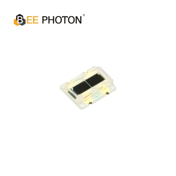
Si PIN Photodiode Array PDCA02-102
The PDCA02-102 is a high-performance Si PIN Photodiode Array designed for precision optical measurement and alignment systems. Engineered by Bee Photon, this 2-segment photodiode delivers a wide spectral response range from 400nm to 1100nm, covering the entire visible light spectrum into the near-infrared (NIR) region.
With its compact COB (Chip on Board) package and resin window, the PDCA02-102 ensures durability and easy integration into compact optical modules. It is specifically optimized for industrial applications where high sensitivity and fast response times are critical.
FAQ
What is a good photosensitivity A/W value for silicon photodiodes at 1064 nm?
Typical values range from 0.38 to 0.45 A/W on standard parts, but with light trapping and optimized thickness, you can reach 0.55-0.58 A/W or slightly higher in real devices. It depends heavily on exact construction.
How does responsivity relate to Si PIN efficiency?
Responsivity (A/W) is basically the practical outcome of quantum efficiency combined with photon energy. Higher QE directly drives higher photosensitivity A/W. In PIN structures, the wide depletion region helps achieve better collection efficiency than simple PN diodes.
Can I improve existing silicon photodiodes or do I need new ones?
You can gain some improvement through better biasing, optical coupling, and AR coatings on the system level. For big jumps, especially at challenging wavelengths, selecting a purpose-optimized Si PIN photodiode usually gives the best and most repeatable results.
Does higher photosensitivity always mean better system performance?
Not automatically. You have to balance it against bandwidth, noise, and capacitance. A device with great A/W but high dark current might underperform in low-light, high-speed scenarios compared to a more balanced part.