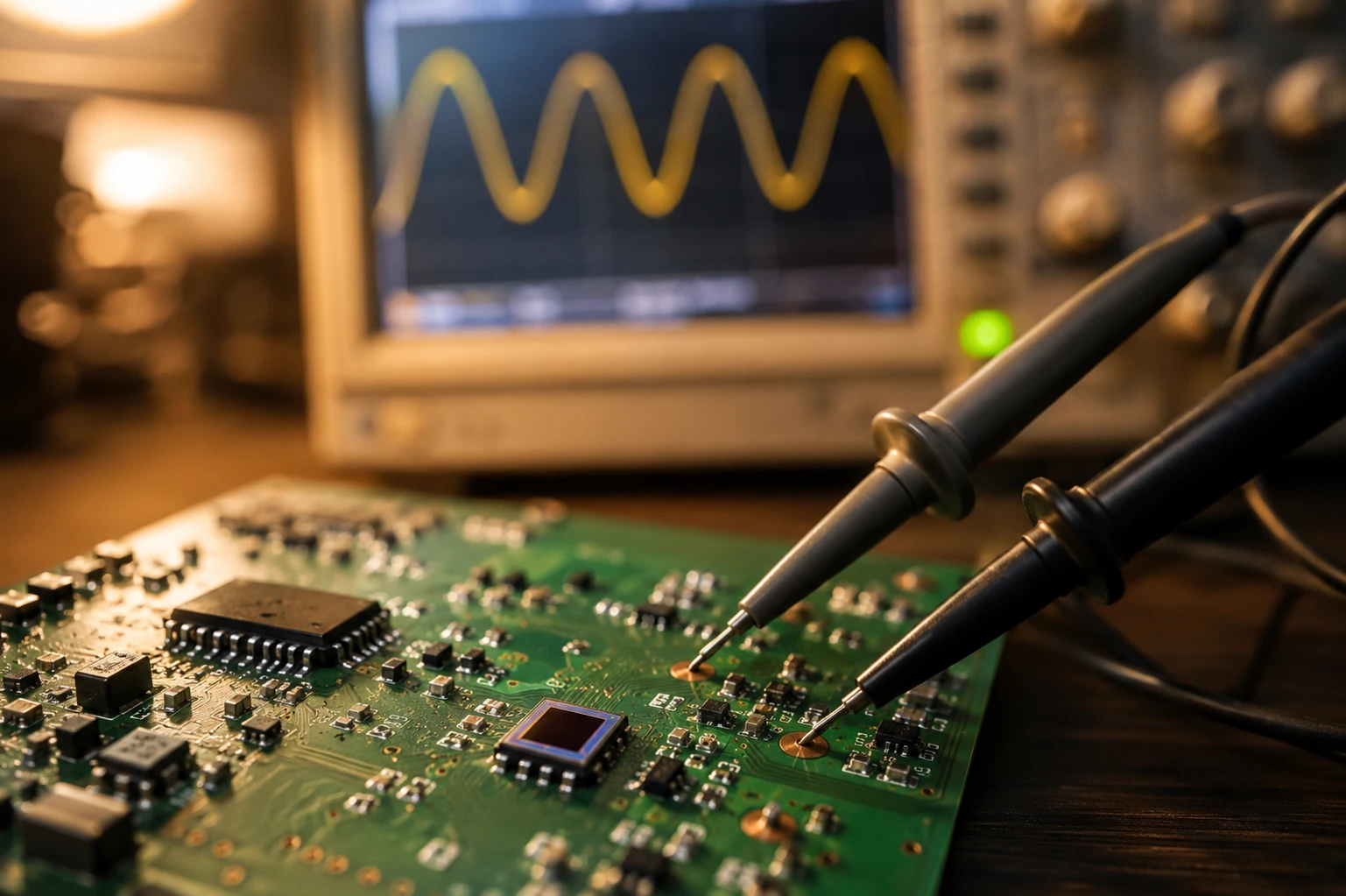
If you have ever spent a long night in the lab debugging a custom high-speed scan head, you probably know this nightmare. You power up your board, hook up the laser, and check your oscilloscope, expecting a clean position feedback signal. Instead, you are greeted by a beautiful, clean, 12 MHz sine wave. Your circuit is screaming in self-excitation. You have built an oscillator instead of a stable transimpedance amplifier for photodiodes.
Or maybe you got the circuit stable by slapping a massive capacitor across the feedback resistor, but now your 3dB bandwidth is so sluggish that your galvo scanner is dragging its feet, causing horrible rounding at the corners of your laser marks. Getting a high-speed transimpedance amplifier for photodiodes to behave in a fast optical feedback loop is one of the most frustrating analog design challenges. You are trying to balance transimpedance gain, high-frequency noise, phase margin, and bandwidth all at once.
In this deep-dive guide, we will walk through how to stop chasing your tail and actually solve these stability and bandwidth bottlenecks. We won’t just look at textbook equations. We will dive into the real-world math of matching your op-amp with your detector chip, focusing on how chip-level impedance and capacitance matching can save your design. If you want to build a rock-solid transimpedance amplifier for photodiodes that actually works on the first spin, you have come to the right place.
Understanding Loop Instability in an Op Amp Photodiode Interface Circuit
To build a reliable transimpedance amplifier for photodiodes, we first need to look at what is actually happening at the input of our op amp photodiode interface circuit.
Let’s face it: on paper, a photodiode is just a perfect current source that converts photons into electrons. In reality, it is a messy combination of a current source, a junction capacitance (C_j), a massive shunt resistance (R_sh), and some parasitic series resistance. When you connect this sensor to the inverting input of your op-amp, that junction capacitance does not just disappear. It adds directly to the op-amp’s own input capacitance (both common-mode and differential), creating a total input capacitance (C_in).
This total input capacitance is the primary enemy of a stable transimpedance amplifier for photodiodes. Why? Because C_in, alongside your feedback resistor (R_f), forms a low-pass filter in your feedback path. This filter introduces a pole in your loop gain transfer function at a frequency we’ll call f_p:
f_p = 1 / (2 * pi * R_f * C_in)
At this pole frequency, the feedback signal starts lagging behind. By the time the signal travels through the op-amp and back through the feedback network, that lag can approach 90 degrees. If you combine that with the op-amp’s own internal high-frequency phase shift, your total loop phase shift hits 180 degrees at the unity-gain crossover frequency. Suddenly, your negative feedback has turned into positive feedback. Your transimpedance amplifier for photodiodes starts oscillating, and your debug session is officially ruined.
To prevent this, you have to add a small feedback capacitor (C_f) in parallel with R_f. This capacitor introduces a feedback zero that counteracts the phase lag caused by C_in. But here is the catch: when you increase C_f to stabilize your transimpedance amplifier for photodiodes, you pull down the closed-loop bandwidth of your system. The closed-loop 3dB bandwidth of a compensated transimpedance amplifier for photodiodes is roughly:
f_3dB = sqrt( GBW / (2 * pi * R_f * C_in) )
Look closely at that equation. The bandwidth is inversely proportional to the square root of C_in. If your photodiode chip has a huge junction capacitance, your bandwidth is going to tank. To keep your feedback loop fast and stable, you need to minimize C_in. Since you cannot change the op-amp’s internal input capacitance, the only way to win this game is to optimize the sensor’s junction capacitance. This is why selecting the right photodiode chip is the absolute foundation of designing a high-speed transimpedance amplifier for photodiodes.
Si PIN photodiodes for Galvo PDC-C2928-NIR-B
Optimize scanning with our 940nm PIN photodiode chip, PDC-C2928-NIR-B. This 940nm PIN photodiode chip ensures precise galvo position sensing and low noise.
Matching Photodiode Capacitance at the Chip Level: The Key to TIA Design Photodiode Success
When you are working on a high-precision B2B project, like a high-speed laser marking scanner or a galvanometer position feedback loop, you cannot just throw in a generic catalog photodiode and hope for the best. To build a successful transimpedance amplifier for photodiodes, you need to match your sensor’s electrical characteristics directly to your amplifier’s performance. Let’s look at how specialized silicon PIN photodiodes change the game.
For near-infrared (NIR) laser systems operating at 940nm, the Si PIN photodiodes for Galvo PDC-C2928-NIR-B from BeePhoton is a prime example of a chip optimized for fast optical feedback. If you are designing a high-speed transimpedance amplifier for photodiodes, this chip gives you an exceptional starting point. It features an ultra-low dark current of just 5 pA at 10mV bias, which keeps your noise floor incredibly quiet. More importantly, its junction capacitance is tightly controlled. When you apply a reverse bias, the capacitance drops even further, allowing you to maximize the bandwidth of your transimpedance amplifier for photodiodes without triggering self-excitation.
What if you are working on a tighter budget? You don’t always need to pay a premium for custom high-end silicon if you are building a cost-sensitive industrial marker. For 920nm systems, the Si PIN photodiodes for Galvo PDC-C2929 is an amazing fit. It keeps your bill of materials low while still offering a very stable 70 pF junction capacitance. When paired with a properly compensated transimpedance amplifier for photodiodes, this budget-friendly chip can easily deliver several megahertz of clean feedback bandwidth.
For ultra-high-end applications, single-channel detectors sometimes won’t cut it. If you are building a sub-microradian galvo scanner, you probably need a segmented sensor for differential angular tracking. This is where the Si PIN photodiodes for Galvo PDC-2C3432-NIR-B shines. This segmented PIN photodiode chip features a dual-segment fan-shaped design on a single silicon substrate. Why is this a massive deal for your transimpedance amplifier for photodiodes? Because the segments are fabricated on the exact same wafer, their junction capacitances and shunt resistances match perfectly. If you run a differential transimpedance amplifier for photodiodes layout, any minor capacitance drift or thermal noise is treated as common-mode. It cancels out beautifully in your differential stage, preventing your loop from drifting even in hot industrial workshops.
Selecting the Right Op-Amp: Crucial Parameters for Your Transimpedance Amplifier for Photodiodes
Now that we have looked at the photodiode chip, let’s talk about the other half of the equation: the op-amp. Selecting the wrong op-amp for your transimpedance amplifier for photodiodes will doom your project from the start, no matter how great your silicon sensor is. Let’s break down the key specifications you need to watch out for.
1. Input Bias Current (I_b)
If you are building a high-gain transimpedance amplifier for photodiodes, you must pay attention to the op-amp’s input bias current. This current flows out of (or into) the op-amp’s input pins and through your feedback resistor R_f, creating a parasitic DC offset voltage:
V_offset = I_b * R_f
If you use a bipolar op-amp with microamps of bias current, your transimpedance amplifier for photodiodes will saturate its output before you even turn on your laser! To avoid this, you need an op-amp with FET or CMOS inputs. These devices have input bias currents in the picoamp or even femtoamp range. This ensures your transimpedance amplifier for photodiodes has near-zero offset, maintaining a clean, wide dynamic range for your optical feedback loop.
2. Gain Bandwidth Product (GBW)
To get high closed-loop bandwidth out of your transimpedance amplifier for photodiodes, you need an op-amp with a massive Gain Bandwidth Product. Many engineers assume that if they need a 5 MHz closed-loop bandwidth, a 10 MHz GBW op-amp is plenty. That is a huge mistake!
Because of the noise gain peaking effect, the loop gain of a transimpedance amplifier for photodiodes rolls off much faster than a standard non-inverting amplifier. To achieve a stable, flat response at 5 MHz with a decent transimpedance gain, you often need an op-amp with a GBW of 100 MHz or even higher. When designing a high-speed transimpedance amplifier for photodiodes, always overshoot on your GBW budget.
3. Input Capacitance (C_cm and C_diff)
As we discussed earlier, the total input capacitance C_in is the root cause of loop instability in a transimpedance amplifier for photodiodes. C_in is the sum of the photodiode junction capacitance C_j and the op-amp’s own input capacitance:
C_in = C_j + C_cm + C_diff
Where C_cm is the common-mode input capacitance and C_diff is the differential input capacitance of the op-amp. If you choose an op-amp with 10 pF of input capacitance, you are adding a heavy load to your feedback loop before you even connect the sensor. For a high-performance transimpedance amplifier for photodiodes, look for op-amps with extremely low input capacitance—ideally below 3 pF. Combined with a low-capacitance photodiode chip like the PDC-C2928-NIR-B, this keeps C_in low and your bandwidth high.
4. Input Voltage Noise (e_n) and Current Noise (i_n)
At high frequencies, the noise of a transimpedance amplifier for photodiodes is dominated by the op-amp’s input voltage noise e_n multiplying with the input capacitance C_in. This is the dreaded noise gain peaking. A larger input capacitance not only threatens the stability of your transimpedance amplifier for photodiodes, but it also spikes your high-frequency noise floor. This is why a low-noise transimpedance amplifier for photodiodes requires a low-noise op-amp paired with a low-capacitance detector chip.
Deep Dive: How Junction Capacitance Dictates TIA Stability and Bandwidth
Let’s put the textbook equations to work and look at a concrete design example. We will build a transimpedance amplifier for photodiodes with a transimpedance gain of 10 kOhm (R_f = 10,000 Ohms). We will pair this circuit with a high-speed FET-input op-amp like the OPA656, which has a Gain Bandwidth Product (GBW) of 230 MHz and a total input capacitance (C_amp = C_cm + C_diff) of 2.8 pF.
We want to compare how three different photodiode chips from BeePhoton behave in this exact transimpedance amplifier for photodiodes setup. We will calculate the required feedback capacitor (C_f) for a stable, maximally flat Butterworth response, and the resulting closed-loop 3dB bandwidth (f_3dB).
The formulas we will use for our transimpedance amplifier for photodiodes design are:
C_in = C_j + C_amp
C_f = sqrt( C_in / (2 * pi * R_f * GBW) )
f_3dB = sqrt( GBW / (2 * pi * R_f * C_in) )
Let’s do the math for each sensor chip.
Case A: Budget-Friendly 920nm System (PDC-C2929)
The PDC-C2929 is a highly cost-effective 920nm silicon PIN photodiode with a junction capacitance (C_j) of 70 pF. Let’s see how it matches our transimpedance amplifier for photodiodes:
Total input capacitance:
C_in = 70 pF + 2.8 pF = 72.8 pF
Required feedback capacitor (C_f) for our transimpedance amplifier for photodiodes:
C_f = sqrt( 72.8 * 10^-12 / (2 * 3.14159 * 10,000 * 230 * 10^6) )
C_f = sqrt( 72.8 * 10^-12 / (1.445 * 10^13) )
C_f = sqrt( 5.038 * 10^-24 )
C_f = 2.24 pF (we can use a standard 2.2 pF ceramic capacitor)
Closed-loop bandwidth (f_3dB) of this transimpedance amplifier for photodiodes:
f_3dB = sqrt( 230 * 10^6 / (2 * 3.14159 * 10,000 * 72.8 * 10^-12) )
f_3dB = sqrt( 230 * 10^6 / (4.574 * 10^-6) )
f_3dB = sqrt( 5.028 * 10^13 )
f_3dB = 7.09 MHz
Case B: High-Performance 940nm System (PDC-C2928-NIR-B)
The PDC-C2928-NIR-B is optimized for high-precision, low-drift 940nm loops. It features a junction capacitance (C_j) of 125 pF at zero bias. Let’s calculate its performance in our transimpedance amplifier for photodiodes:
Total input capacitance:
C_in = 125 pF + 2.8 pF = 127.8 pF
Required feedback capacitor (C_f) for stability:
C_f = sqrt( 127.8 * 10^-12 / (2 * 3.14159 * 10,000 * 230 * 10^6) )
C_f = sqrt( 127.8 * 10^-12 / (1.445 * 10^13) )
C_f = sqrt( 8.844 * 10^-24 )
C_f = 2.97 pF (a 3.0 pF standard capacitor works beautifully)
Closed-loop bandwidth (f_3dB) of our high-precision transimpedance amplifier for photodiodes:
f_3dB = sqrt( 230 * 10^6 / (2 * 3.14159 * 10,000 * 127.8 * 10^-12) )
f_3dB = sqrt( 230 * 10^6 / (8.03 * 10^-6) )
f_3dB = sqrt( 2.864 * 10^13 )
f_3dB = 5.35 MHz
This provides an incredibly stable 5.35 MHz feedback loop with single-digit picoamp thermal drift.
Case C: Segmented Position Feedback System (PDC-2C3432-NIR-B)
The PDC-2C3432-NIR-B is a dual-segment fan-shaped chip designed for differential angular tracking. Each segment features a lower junction capacitance of roughly 60 pF due to the split active area. Let’s calculate the performance for one of the channels in this differential transimpedance amplifier for photodiodes circuit:
Total input capacitance:
C_in = 60 pF + 2.8 pF = 62.8 pF
Required feedback capacitor (C_f):
C_f = sqrt( 62.8 * 10^-12 / (2 * 3.14159 * 10,000 * 230 * 10^6) )
C_f = sqrt( 62.8 * 10^-12 / (1.445 * 10^13) )
C_f = sqrt( 4.346 * 10^-24 )
C_f = 2.08 pF (a standard 2.0 pF or 2.2 pF capacitor is perfect)
Closed-loop bandwidth (f_3dB) for each segment of this differential transimpedance amplifier for photodiodes:
f_3dB = sqrt( 230 * 10^6 / (2 * 3.14159 * 10,000 * 62.8 * 10^-12) )
f_3dB = sqrt( 230 * 10^6 / (3.946 * 10^-6) )
f_3dB = sqrt( 5.828 * 10^13 )
f_3dB = 7.63 MHz
Because both channels of this segmented PIN chip share the same silicon, their C_j values are closely matched, keeping the delay times identical across both arms of your differential transimpedance amplifier for photodiodes circuit.
Comparison Table: TIA Design Photodiode Matching (R_f = 10 kOhm, GBW = 230 MHz, C_amp = 2.8 pF)
| Photodiode Chip Model | Target Wavelength | Junction Capacitance (C_j) | Required Feedback Cap (C_f) | Resulting Closed-Loop Bandwidth (f_3dB) | Ideal Applications |
|---|---|---|---|---|---|
| PDC-C2929 | 920 nm | 70 pF | 2.24 pF | 7.09 MHz | Cost-effective scanners, entry-level markers |
| PDC-C2928-NIR-B | 940 nm | 125 pF | 2.97 pF | 5.35 MHz | High-precision laser marking, low-noise systems |
| PDC-2C3432-NIR-B | 940 nm (NIR) | 60 pF (per segment) | 2.08 pF | 7.63 MHz | Segmented angular tracking, differential galvo loops |
As you can see, a smaller junction capacitance directly translates to a smaller required stabilizing capacitor C_f, which in turn gives your transimpedance amplifier for photodiodes a much higher bandwidth limit.
Si PIN photodiodes for Galvo PDC-2C3432-NIR-B
The PDC-2C3432-NIR-B is a specialized segmented PIN photodiode chip engineered for precise differential position feedback in high-speed galvanometer scanners. Integrating this dual-channel segmented PIN photodiode chip allows systems to obtain accurate angular tracking with minimal signal noise.
Practical Debugging: How to Tame an Oscillating Current to Voltage Converter Scanner
If you are debugging on the bench and your transimpedance amplifier for photodiodes is still acting like an oscillator, don’t throw your board in the trash just yet. Let’s look at some real-world troubleshooting steps that I’ve used on many late nights to stabilize a stubborn current to voltage converter scanner circuit.
1. Strip the Ground Plane Under the Inverting Input Pin
This is one of the most common layout mistakes. When you design a PCB, you’re taught to pour solid ground planes everywhere to minimize noise. But if you run a solid ground plane directly under the inverting input pin of your op-amp and the trace connecting it to the photodiode, you are creating a parasitic capacitor to ground.
This parasitic capacitance adds directly to your C_in, which immediately destabilizes your transimpedance amplifier for photodiodes. In your next PCB revision, strip out the ground and power planes under that trace and the inverting input pin. For your current prototype, you can carefully scrape away the PCB copper around the inverting node with an X-Acto knife to see if the oscillation subsides.
2. Double-Check Your Feedback Resistor Parasitics
Every physical resistor has a tiny parasitic parallel capacitance. For standard 0603 or 0805 surface-mount resistors, this is usually around 0.1 pF to 0.2 pF. While this sounds tiny, in a high-speed transimpedance amplifier for photodiodes, that parasitic capacitance acts as a small stabilizing feedback capacitor.
But if you are using multiple resistors in series to get your desired R_f, or if your layout has long traces running parallel to the resistor body, you might end up with too much parasitic capacitance, which will slow down your transimpedance amplifier for photodiodes. Conversely, if you don’t have enough capacitance, the circuit will oscillate. Always place your feedback capacitor C_f directly over your feedback resistor R_f with the shortest possible traces.
3. Apply a Reverse Bias to Reduce Junction Capacitance
If you need more bandwidth and cannot change your photodiode, you can apply a reverse bias voltage across your sensor. Reverse biasing widens the depletion region of the silicon PIN junction, which significantly lowers its junction capacitance (C_j).
For example, applying a stable 5V or 10V reverse bias can drop your sensor’s capacitance by 50% or more, allowing you to use a much smaller C_f and achieve a much higher cutoff frequency in your transimpedance amplifier for photodiodes.
However, there is a catch: reverse biasing increases the dark current of your silicon photodiode. In low-quality chips, this dark current drifts wildly with temperature, showing up as physical drift in your galvo scanner position. To avoid this, you must source a high-quality chip with extremely low dark current leakage, such as the Si PIN photodiodes for Galvo PDC-C2928-NIR-B. Its ultra-clean silicon structure limits dark current to single-digit picoamperes, allowing you to apply a reverse bias to speed up your transimpedance amplifier for photodiodes without suffering from horrible thermal drift.
4. Optimize the Layout of Your Power Supply Decoupling
High-speed op-amps are extremely sensitive to power supply impedance. If your decoupling capacitors are placed too far from the op-amp supply pins, the amplifier will oscillate. Ensure you have a 0.1 uF ceramic capacitor placed as close as humanly possible to the supply pins of your op-amp, backed by a 10 uF tantalum capacitor. A clean, low-impedance power source is mandatory for any stable transimpedance amplifier for photodiodes.
Case Study: Eliminating Mirror Jitter in a 940nm Galvo Scanner Feedback Loop
Let’s look at how these chip-level impedance and capacitance matching solutions play out in a real B2B manufacturing scenario. A couple of years ago, we worked with a team that was designing an automated laser marking machine for medical implants. The scanner used a 940nm near-infrared laser, and they were experiencing severe line jitter and feathering whenever the galvanometer scanned at speeds above 500 mm/s.
During testing, they noticed a high-frequency, 500 kHz ringing on the position feedback analog signals. Their original position sensor circuit used a generic, off-the-shelf 940nm photodiode with a nominal junction capacitance of 180 pF, paired with a standard op-amp in their transimpedance amplifier for photodiodes stage. Because the junction capacitance of the generic sensor was so high and varied across different wafer lots, the stabilizing feedback capacitor C_f they chose was either too small (causing ringing and oscillation) or too large (causing slow response times).
To solve this bottleneck, we recommended they redesign their feedback board around a high-stability, low-capacitance photodiode chip and optimize their transimpedance amplifier for photodiodes parameters. They made the following modifications:
- Upgraded the Photodiode: They replaced the generic 180 pF sensor with BeePhoton’s Si PIN photodiodes for Galvo PDC-C2928-NIR-B. This immediate swap dropped their sensor’s junction capacitance down to 125 pF at zero bias. Thanks to the wafer-level consistency of the BeePhoton chip, the junction capacitance remained perfectly uniform across all production batches, ensuring that a single TIA design worked for every unit.
- Applied a 5V Reverse Bias: To push their loop bandwidth even higher, they applied a stable 5V reverse bias to the PDC-C2928-NIR-B chip. This dropped the junction capacitance from 125 pF down to a tiny 50 pF. Because of the ultra-clean silicon structure of the BeePhoton chip, the dark current remained at a negligible 5 pA, meaning they suffered zero thermal drift during long operating runs.
- Optimized the TIA Loop: With a total input capacitance C_in of just 52.8 pF (sensor plus op-amp capacitance), they were able to reduce the feedback capacitor C_f in their transimpedance amplifier for photodiodes down to 1.9 pF.
- PCB Layout Adjustments: They scraped the ground plane from directly underneath the feedback resistor and the op-amp’s inverting input node to eliminate parasitic capacitive loading.
The results were immediate and dramatic. The 500 kHz ringing on the feedback signal was completely eliminated, and the closed-loop feedback bandwidth of their transimpedance amplifier for photodiodes jumped from a sluggish 150 kHz to over 800 kHz. Jitter on the laser marker dropped by more than 15 dB. The medical implants were marked with razor-sharp precision, even at maximum scanning speeds. The manufacturer was able to double their daily production throughput while completely eliminating scrap parts caused by blurry feedback loops.
Si PIN photodiodes for Galvo PDC-C2929
The PDC-C2929 is a budget-friendly 920nm silicon PIN photodiode chip. This 920nm silicon PIN photodiode offers stable, cost-effective scanner position tracking.
Frequently Asked Questions About TIA Design Photodiode Matching
Q1: Why does my transimpedance amplifier for photodiodes oscillate when I use a larger photodiode chip?
A: A larger photodiode chip has a larger active area, which directly increases its junction capacitance (C_j). When this high capacitance is connected to your op-amp’s inverting input, it forms a low-pass filter with your feedback resistor (R_f). This filter creates a pole in the loop transfer function, introducing a significant phase lag. If this phase lag hits 90 degrees before the loop gain drops below unity, the negative feedback turns into positive feedback, causing your transimpedance amplifier for photodiodes to self-oscillate. To stabilize it, you must add a feedback capacitor (C_f) or select a lower-capacitance chip like the PDC-C2929.
Q2: How does reverse biasing stabilize a transimpedance amplifier for photodiodes?
A: Reverse biasing a silicon PIN photodiode increases the thickness of its depletion region. Since capacitance is inversely proportional to the depletion width, applying a reverse bias voltage significantly lowers the junction capacitance (C_j). Lowering C_j directly reduces the total input capacitance (C_in) of your transimpedance amplifier for photodiodes. This shifts the loop pole to a much higher frequency, giving you a better phase margin and allowing you to achieve a much higher closed-loop bandwidth with a smaller stabilizing feedback capacitor (C_f).
Q3: Why is dark current important when designing a fast transimpedance amplifier for photodiodes?
A: When you apply a reverse bias to speed up your transimpedance amplifier for photodiodes, you also increase the sensor’s leakage current, known as dark current. If you use a cheap, low-quality sensor, this dark current will increase exponentially as your industrial system heats up during operation. This climbing dark current creates a moving DC offset voltage at the output of your transimpedance amplifier for photodiodes, which look like actual physical mirror movement to your controller, causing your laser beam to drift. Sourcing a high-quality, low-drift chip like BeePhoton’s PDC-C2928-NIR-B keeps dark current to a rock-solid 5 pA, preventing thermal drift from ruining your system’s accuracy.
Elevate Your Optical Feedback Loops Today
Are you tired of chasing self-excitation oscillations and sacrificing your loop bandwidth to keep your laser scanners stable? Building a stable, high-speed transimpedance amplifier for photodiodes shouldn’t be a guessing game of trial and error on the bench.
The key to unlocking sub-microradian laser tracking and megahertz-level feedback lies in pairing your op-amp with high-stability, low-capacitance photodiode chips designed specifically for industrial environments. By matching your amplifier circuits with premium silicon from BeePhoton, you can eliminate phase delays, slash your high-frequency noise floor, and guarantee consistent wafer-level performance across thousands of production units.
Whether your system requires the advanced, dual-channel differential tracking of our Si PIN photodiodes for Galvo PDC-2C3432-NIR-B, the ultra-stable, high-shunt performance of our Si PIN photodiodes for Galvo PDC-C2928-NIR-B, or the cost-effective reliability of our Si PIN photodiodes for Galvo PDC-C2929 for budget-conscious scanner designs, we have the wafer-level engineering expertise to help you succeed.
Don’t let unstable feedback loops slow down your product development. Stop fighting your noise floor and contact our team of optical specialists today at info@photo-detector.com or head over to our contact page to request custom evaluation samples, discuss your specific optical layout, or receive a fast, direct B2B pricing quote for your next production run!