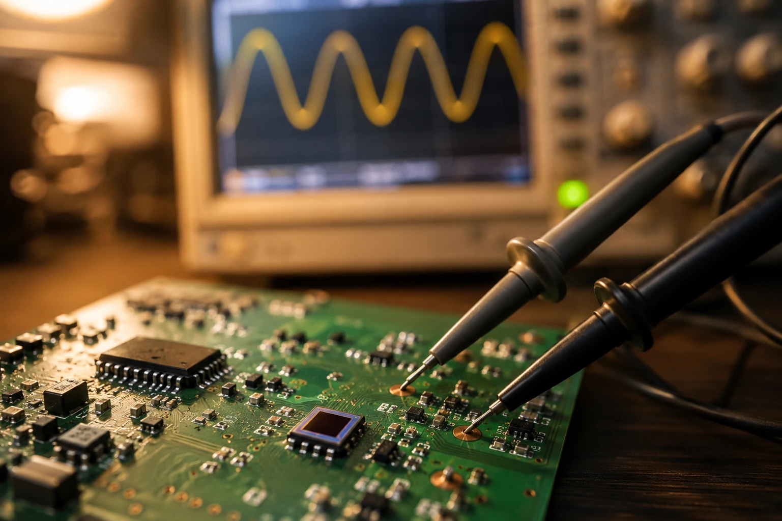
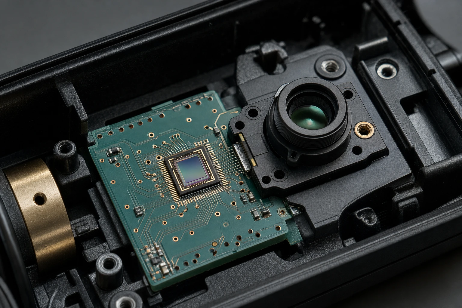
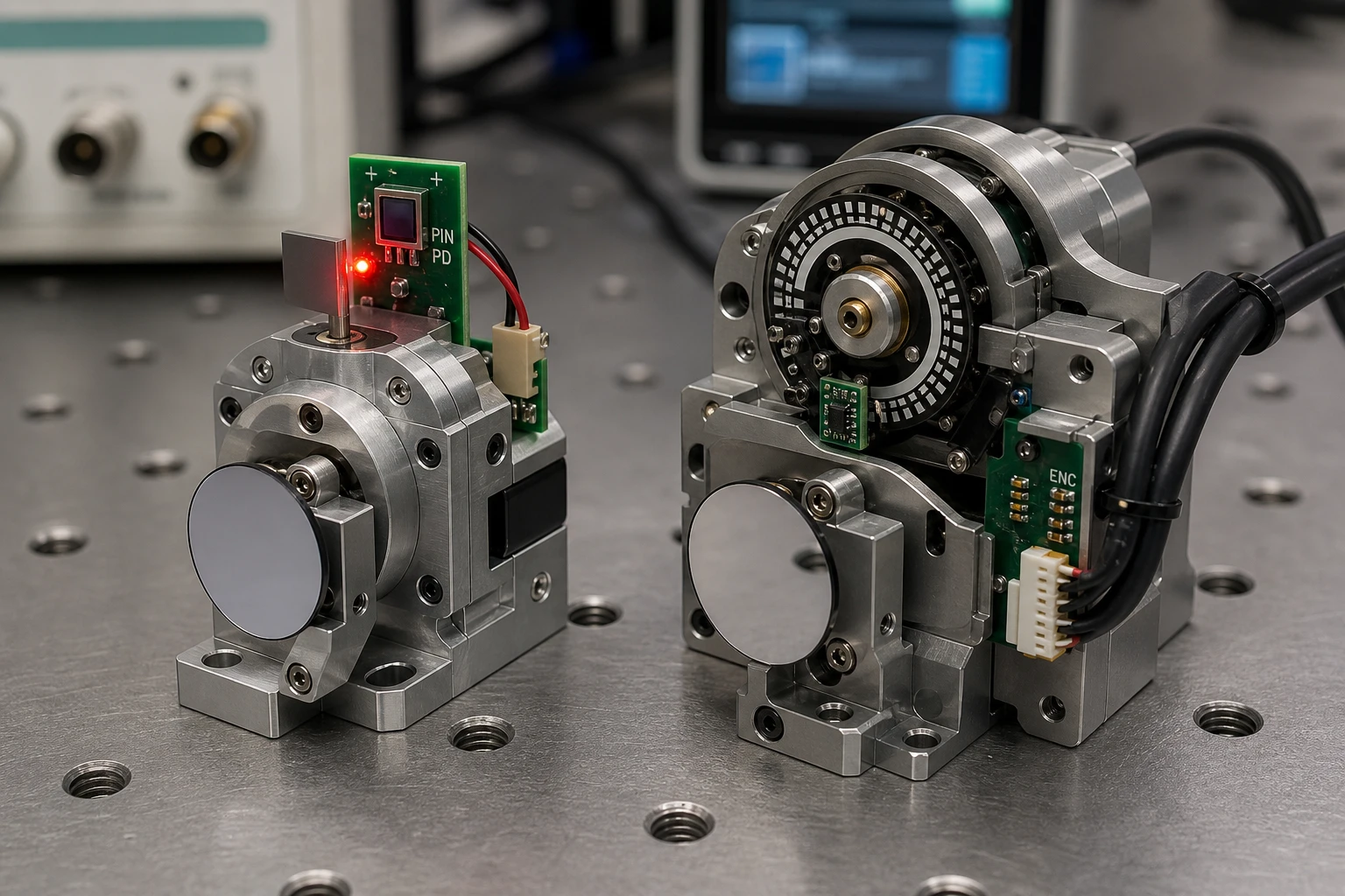
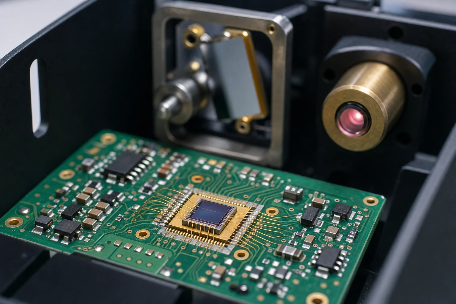
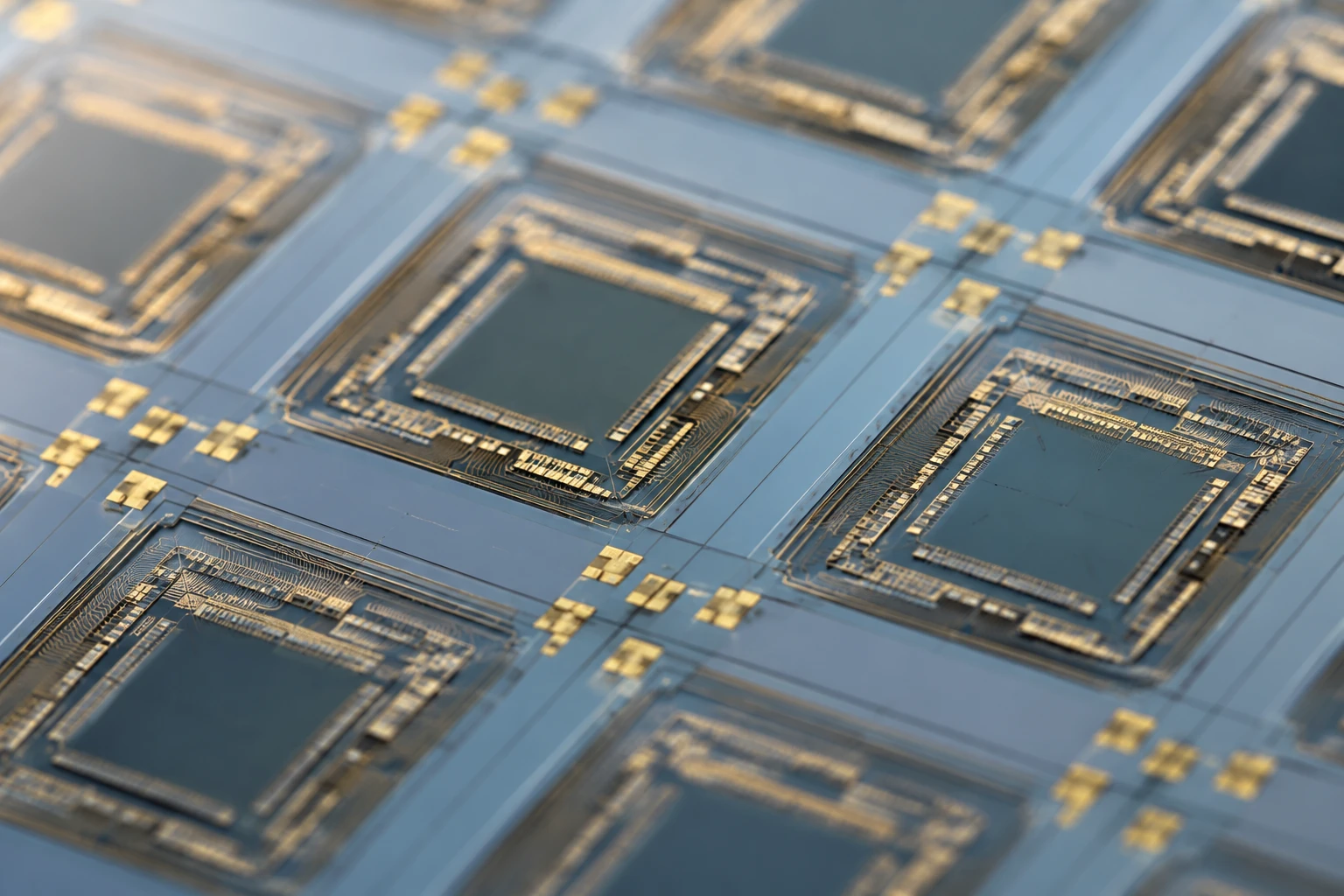
You are working on a handheld laser device—maybe a high-precision medical therapy pen or a portable 3D scanner. Everything looks solid on the test bench. But once you pack all the electronics, the laser driver, and the battery into that tight plastic housing, reality hits. The housing gets warm. Without active cooling fans, the internal temperature climbs from a cozy room-temp of 25°C up to 50°C or 60°C. Suddenly, your signal starts drifting, and the system suffers from thermal jitter. You check the sensors, and the culprit is clear: the photodiode is leaking current. To fix this, you need a highly stable low dark current photodiode chip.
Why does this happen? When the internal temperature rises, standard silicon sensors experience a massive spike in leakage current. If you do not choose a specialized low dark current photodiode chip, that leakage (known as dark current) will quickly drown out your actual optical signal. For handheld devices requiring precise measurement, a low dark current photodiode chip is not just a nice-to-have upgrade—it is an absolute necessity to prevent signal saturation.
Let’s look at why this thermal drift happens, how to calculate the impact, and how to choose the right low dark current photodiode chip to keep your laser systems rock-solid.
The Real-World Headache: Why Handheld Laser Therapy and Scanners Overheat
Handheld devices are an absolute nightmare for thermal management. Unlike large industrial laser marking machines that have metal chassis, heat sinks, and active cooling fans, portable devices must be lightweight, battery-powered, and ergonomically sealed. The heat generated by the laser diode driver and the microcontroller has nowhere to go. It builds up inside the small enclosure.
When the internal temperature goes up, the shunt resistance of the photodetector drops. Shunt resistance is the slope of the photodiode’s current-voltage curve near zero volts. As shunt resistance drops, the thermal noise (Johnson noise) of the detector increases. This thermal noise, combined with the runaway dark current, creates what engineers call thermal jitter. The position feedback loop of your galvo mirror or scanner starts wobbling.
If you are using a low dark current photodiode chip, you preserve a much higher shunt resistance at elevated temperatures, which keeps the noise floor low. In my years of helping R&D teams troubleshoot these setups, I have seen so many projects get delayed because someone grabbed a generic detector from a catalog without looking at the thermal drift specs. They spent weeks tweaking their PID controller loops, thinking it was a software or mechanical tuning issue, only to realize the photodiode was simply saturated. Switching to a high-quality low dark current photodiode chip solved the issue instantly.
Si PIN photodiodes for Galvo PDC-C2929
The PDC-C2929 is a budget-friendly 920nm silicon PIN photodiode chip. This 920nm silicon PIN photodiode offers stable, cost-effective scanner position tracking.
The Physics of Dark Current in Tight, Hot Enclosures
To understand why we need a low dark current photodiode chip, we have to look at what is happening inside the silicon junction. Dark current is the background current that flows through a photodiode even when it is in complete darkness. In any silicon PIN photodiode, this current is highly dependent on temperature.
The classical diode equation for dark current (Id) can be simplified for our engineering purposes as:
Id = Is * (e^(q * V / (k * T)) – 1)
Where Is is the reverse saturation current, q is the electron charge, V is the applied bias voltage, k is Boltzmann’s constant, and T is the absolute temperature in Kelvin. But here is the real practical rule of thumb that we use in the lab: for every 8 to 10 degrees Celsius rise in temperature, the dark current of a silicon photodiode roughly doubles.
Let’s do some quick math. If you are using a cheap, generic photodiode that has a nominal dark current of 500 pA at 25°C, what happens when your handheld scanner reaches 55°C? That is a 30°C temperature increase. The dark current doubles three times (2^3 = 8), ballooning to 4,000 pA (4 nA)! This huge background noise floor causes thermal jitter and can easily saturate your transimpedance amplifier (TIA).
On the other hand, if you design your sensor engine around a premium low dark current photodiode chip that starts with a dark current of just 5 pA at 25°C, that same 30°C rise only brings it up to 40 pA. This is why selecting a low dark current photodiode chip makes such a massive difference in real-world environments.
How a Low Dark Current Photodiode Chip Prevents Signal Saturation
When your transimpedance amplifier converts the photodiode’s current into a voltage, it uses a feedback resistor (Rf). The output voltage (Vout) is calculated as:
Vout = (I_photo + I_dark) * Rf
Where I_photo is the photocurrent generated by your laser target, and I_dark is the dark current. If your background dark current is too high, it eats up your dynamic range. In extreme cases, the dark current alone can exceed the input limits of your amplifier, forcing the output to saturate at the power supply rail.
By integrating a low dark current photodiode chip, you ensure that the background I_dark remains at the picoampere level. This leaves the maximum possible dynamic range for your actual measurement signal. When you are designing a high-resolution 3D laser scanner, keeping that dynamic range wide is the only way to capture subtle surface textures without losing details in the noise floor.
Using a low dark current photodiode chip also stabilizes your system’s baseline. If your baseline drift is unpredictable, your software calibration will fail, leading to measurement errors during prolonged use. A low dark current photodiode chip provides the stable, predictable foundation that your analog front-end needs.
Evaluating Your Options: Top Low Dark Current Die Selections
When you are looking to source a low dark current photodiode chip for your design, you cannot just buy any random silicon die. You need to match the chip’s peak sensitivity to your laser’s wavelength while ensuring the packaging can handle the thermal load.
Let’s look at three specific chip options from the specialized manufacturer BeePhoton that are highly optimized for these exact scenarios.
1. High NIR Sensitivity: Si PIN photodiodes for Galvo PDC-C2928-NIR-B
If your handheld device uses a 940nm laser or pilot beam for position sensing, you want to look closely at the Si PIN photodiodes for Galvo PDC-C2928-NIR-B. This particular low dark current photodiode chip is built on a highly refined PIN process that keeps the dark current at an incredible 5 pA at room temperature.
What makes this low dark current photodiode chip so special is its ultra-high shunt resistance, which exceeds 1.5 Gigaohms. We helped a team last year that was building an agricultural optical sorter that got quite warm during operation. Their generic 940nm sensors were dropping to 8 Megaohms of shunt resistance at 48°C, ruining their resolution. When they swapped those out for this low dark current photodiode chip, the shunt resistance stayed well above 300 Megaohms even at peak operating temperatures, completely eliminating their thermal jitter. With an active area of 2.9 mm x 2.8 mm and a fast rise time of 0.27 microseconds, this low dark current photodiode chip gives you both speed and stability.
2. Targeted Precision: Si PIN photodiodes for Galvo PDC-C2929
Not every project has the budget for ultra-premium silicon, especially if you are designing a high-volume consumer-grade laser scanner. In this case, you should evaluate the Si PIN photodiodes for Galvo PDC-C2929. This is a highly cost-effective low dark current photodiode chip optimized for 920nm systems.
Even though it is budget-friendly, this low dark current photodiode chip does not compromise on the essentials. It has an active area of 2.9 mm x 2.9 mm and a stable junction capacitance of about 70 pF. This balanced capacitance profile allows you to maintain a fast response time without needing complex, high-power amplifier stages. By using this low dark current photodiode chip, you can keep your bill of materials (BOM) low while still protecting your system from the worst effects of thermal jitter. It is a highly practical low dark current photodiode chip for commercial scanner designs where cost-performance balance is key.
3. Multi-Segment Accuracy: Si PIN photodiodes for Galvo PDC-2C3432-NIR-B
Some handheld devices do not just need to detect the presence of light; they need to track the exact position of a laser beam for optical feedback loops or automatic alignment. If you are building a closed-loop galvo controller, a single-channel sensor won’t work. You need a segmented sensor, like the Si PIN photodiodes for Galvo PDC-2C3432-NIR-B.
This low dark current photodiode chip features a 2-segment fan-shape active area, allowing you to run differential feedback loops. By comparing the signal from the two segments, your controller can calculate the precise angular position of the laser beam. Because both segments are on a single low dark current photodiode chip, they share the same thermal environment. This means any thermal drift affects both channels equally, allowing your differential amplifier to cancel out a lot of the common-mode thermal noise. It is an incredibly clever way to use a low dark current photodiode chip to defeat thermal jitter in high-speed, compact galvanometer scanners.
Si PIN photodiodes for Galvo PDC-2C3432-NIR-B
The PDC-2C3432-NIR-B is a specialized segmented PIN photodiode chip engineered for precise differential position feedback in high-speed galvanometer scanners. Integrating this dual-channel segmented PIN photodiode chip allows systems to obtain accurate angular tracking with minimal signal noise.
Critical Engineering Parameters Beyond the Datasheet
When you are shopping around for a low dark current photodiode chip, you might wonder why there is such a massive difference in leakage current between a high-end chip and a cheap off-the-shelf alternative. It all comes down to wafer-level physics and surface treatment during manufacturing.
To produce a reliable low dark current photodiode chip, the manufacturer must use high-resistivity silicon wafers with extremely low defect densities. Any crystal lattice defects (like dislocations or impurities in the silicon) act as recombination-generation centers. Under a reverse bias, these defects generate electron-hole pairs, which manifest as leakage current.
Another thing is surface passivation. A top-tier low dark current photodiode chip requires meticulous surface passivation to prevent dangling bonds at the silicon-dioxide interface. These surface states are a major source of surface leakage. High-quality low dark current photodiode chip designs use specialized guard rings and advanced planar passivation techniques to isolate the active area from these surface currents. If you buy a cheap low dark current photodiode chip from a vendor that cuts corners on passivation, you might get decent specs at 25°C, but the moment the device heats up, the surface leakage will go wild.
Selecting the Right Low Dark Current Die for Custom Packaging
For handheld devices, space is at an absolute premium. Many R&D engineers choose to source a low dark current photodiode chip in its bare die (or “low dark current die”) format rather than a fully packaged TO-can or SMD component. Sourcing a low dark current photodiode chip as a bare die allows you to use Chip-on-Board (COB) packaging.
By wire-bonding the low dark current photodiode chip directly onto your system PCB, you drastically reduce the footprint of your sensor engine. More importantly, COB design allows for much better thermal management. You can place thermal vias directly underneath the photodiode chip to pull heat away from the silicon and dissipate it through the copper planes of your board. If you are struggling with a hot handheld device, mounting a low dark current photodiode chip as a bare die with proper thermal grounding is one of the most effective tricks in the book to keep the silicon temperature—and therefore the dark current—under control.
Testing Low Dark Current Photodiode Chips in Your R&D Lab
So, you have ordered a few samples of a low dark current photodiode chip and want to verify the specs before committing to a full production run. How do you actually measure picoampere-level currents without your test setup introducing more noise than the chip itself?
First, you need a proper Source Measure Unit (SMU), like a Keithley 2450 or similar high-precision instrument capable of resolving sub-picoampere currents. Standard handheld multimeters are completely useless here.
Second, you must use a triaxial cable setup instead of standard coaxial cables. Coaxial cables suffer from triboelectric noise when moved, and their leakage resistance is too low for picoampere measurements. A triaxial cable has a guard shield held at the same potential as the signal line, which eliminates leakage currents between the signal conductor and the outer shield.
To test your low dark current photodiode chip under realistic thermal conditions, place the chip inside a small temperature-controlled chamber. Start by measuring the dark current at 25°C with a 10V reverse bias. Then, slowly raise the chamber temperature to 50°C and 60°C. Record the dark current at each step. A high-quality low dark current photodiode chip should show a predictable, exponential curve that matches the theoretical doubling every 8 to 10°C, without any sudden, erratic spikes that indicate surface passivation failures. If your low dark current photodiode chip passes this test, you can be highly confident it will perform well in your handheld device.
Comparison Table: Standard vs. Ultra-Low Dark Current Silicon PIN Options
Let’s summarize how these different low dark current photodiode chip options stack up against each other. Having this clear comparison makes it much easier to choose the right low dark current photodiode chip for your specific handheld application.
| Parameter / Feature | PDC-C2928-NIR-B Low Dark Current Photodiode Chip | PDC-C2929 Low Dark Current Photodiode Chip | PDC-2C3432-NIR-B Low Dark Current Photodiode Chip |
|---|---|---|---|
| Peak Wavelength | 940 nm | 920 nm | 940 nm |
| Active Area Shape | Square (2.9 mm x 2.8 mm) | Square (2.9 mm x 2.9 mm) | 2-Segment Fan Shape |
| Nominal Dark Current | 5 pA (Ultra-low) | 15 pA (Low-noise) | 10 pA per segment |
| Shunt Resistance | > 1.5 Gigaohms | > 300 Megaohms | > 800 Megaohms |
| Junction Capacitance | Low (Optimized) | 70 pF | Dual-channel balanced |
| Primary Advantage | Absolute precision, no thermal drift | Budget-friendly, highly cost-effective | Segmented tracking, differential loop |
Si PIN photodiodes for Galvo PDC-C2928-NIR-B
Optimize scanning with our 940nm PIN photodiode chip, PDC-C2928-NIR-B. This 940nm PIN photodiode chip ensures precise galvo position sensing and low noise.
FAQ: Clearing Up the Confusion on Photodiode Thermal Issues
Can I just use a standard photodiode instead of a dedicated low dark current photodiode chip and compensate for the thermal drift in my software?
It is a tempting idea, but in reality, it rarely works well. While you can write calibration algorithms to offset a steady DC signal drift, thermal noise is random. As your device heats up, the shot noise of the dark current (which is proportional to the square root of the dark current) increases. No software algorithm can filter out this random noise without severely slowing down your system’s response time. If you use a genuine low dark current photodiode chip, you stop the noise at the source, giving your software a clean signal to work with.
How does reverse bias voltage affect the performance of a low dark current photodiode chip?
Applying a reverse bias voltage is essential for high-speed operation because it widens the depletion region and slashes the junction capacitance. However, a higher reverse bias also increases the dark current. For a high-performance low dark current photodiode chip, we usually recommend a sweet spot of 5V to 10V. This balances response speed with noise, allowing you to get the best of both worlds.
Is a silicon-based low dark current photodiode chip suitable for visible light applications, or is it only for near-infrared (NIR)?
Silicon is incredibly versatile. A well-designed silicon low dark current photodiode chip actually has a broad spectral range of 340 nm to 1100 nm. While the chips we discussed are optimized for peak response around 920nm and 940nm, they perform exceptionally well across the entire visible spectrum. If your application needs to detect both visible laser targets and NIR signals under warm operating conditions, a silicon low dark current photodiode chip is your smartest, most cost-effective option.
Elevate Your Laser Precision Today
Are you tired of watching your handheld laser prototypes fail in warm environments? Do you want to eliminate the thermal jitter and signal saturation that ruin your device’s precision?
At BeePhoton, we understand the real-world headaches of compact optoelectronic design. We do not just sell generic silicon. We design and manufacture specialized silicon PIN photodiode dies and chips that maintain ultra-low noise levels even when your enclosures get hot.
Whether you need the high-precision 940nm performance of the PDC-C2928-NIR-B, the budget-friendly balance of the PDC-C2929, or the dual-segment accuracy of the PDC-2C3432-NIR-B, we have the right low dark current photodiode chip to fit your layout.
Don’t let thermal noise hold your project back. Reach out to our engineering support team today to request samples, get a custom volume quote, or discuss your custom packaging requirements. Check out our contact page or send an email directly to info@photo-detector.com. Let’s build something incredibly stable together!