Selecting the Right Partner for Optical Precision
You are designing a high-precision galvo scan head, and you suddenly realize that standard, off-the-shelf optical components just are not cutting it. They are either too bulky, generate too much dark current under operational heat, or they do not align with your specialized laser wavelengths. If you are a procurement manager or an optical systems engineer, finding a reliable silicon PIN photodiode manufacturer is crucial for your custom OEM/ODM projects [photo-detector.com/]. You need components that fit your board layout perfectly, and you need a partner who can customize the silicon wafer itself.
When you are trying to push the boundaries of scan head integration, you cannot just buy from a general distributor who doesn’t understand wafer physics. You need to work with a dedicated silicon PIN photodiode manufacturer who can offer Chip-on-Board (COB) packaging and specialized active area designs [photo-detector.com/product/segmented-pin-photodiode-chip/]. This guide will walk you through what to look for when selecting a partner like BeePhoton, how wafer-level choices impact your scan head performance, and how to protect your supply chain from costly bottlenecks.
What to Look for in a Silicon PIN Photodiode Manufacturer for Scan Heads
Integrating photodetectors into modern galvo scanners is not just about choosing a part number from a catalog. A premier silicon PIN photodiode manufacturer must possess deep wafer-level customization capabilities. When you work with a direct custom photodetector factory, you gain control over the physical and electrical characteristics of the silicon, which is critical for high-speed laser marking, 3D printing, and LiDAR scan heads.
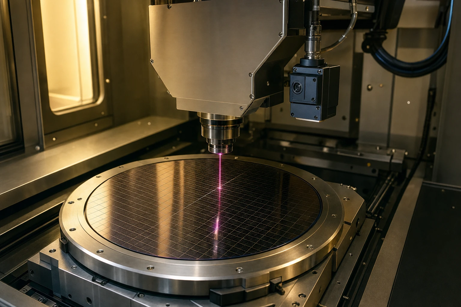
The first thing to evaluate in a silicon PIN photodiode manufacturer is their ability to control the physical properties of the silicon. For instance, in near-infrared (NIR) applications, such as 920nm or 940nm laser scanning, standard silicon has a lower absorption coefficient. A highly specialized silicon PIN photodiode manufacturer can adjust the depletion layer width and the doping profile of the wafer to maximize responsivity at these specific wavelengths.
Let’s look at the basic math behind this. How do we calculate the responsivity of a photodiode? Responsivity (R) is defined as:
R = Ip / Pin
Where Ip is the generated photocurrent in Amperes (A), and Pin is the incident optical power in Watts (W). For a given wavelength (lambda), this is tied to quantum efficiency (QE):
R = (QE * q * lambda) / (h * c)
In this formula, q is the electron charge (1.6 * 10^-19 Coulombs), h is Planck’s constant (6.626 * 10^-34 Joule-seconds), and c is the speed of light (3.0 * 10^8 meters per second). If your silicon PIN photodiode manufacturer doesn’t control the wafer recipe, they cannot optimize the quantum efficiency for your specific laser, meaning your system will struggle with low signal-to-noise ratios.
Why a Standard Silicon PIN Photodiode Manufacturer Fails Modern OEM Designs
Most standard components on the market come in metal-can packages like TO-5 or TO-18. While these are great for simple lab setups, they are terrible for ultra-compact galvo scan heads. A standard catalog-focused silicon PIN photodiode manufacturer will simply point you to their catalog sheet. They won’t alter the lead frame, they won’t offer custom submounts, and they definitely won’t design a segmented chip just for your low-volume production run.
By contrast, an agile silicon PIN photodiode manufacturer understands that modern scan head designs require custom geometries. Whether you need a quadrant photodiode for beam alignment or a dual-segment array to monitor galvo mirror position, you need direct communication with the engineers at a custom photodetector factory. Working with a flexible silicon PIN photodiode manufacturer like BeePhoton lets you customize the shape of the active area to match your scan head’s specific optical path, preventing optical crosstalk and stray light issues.
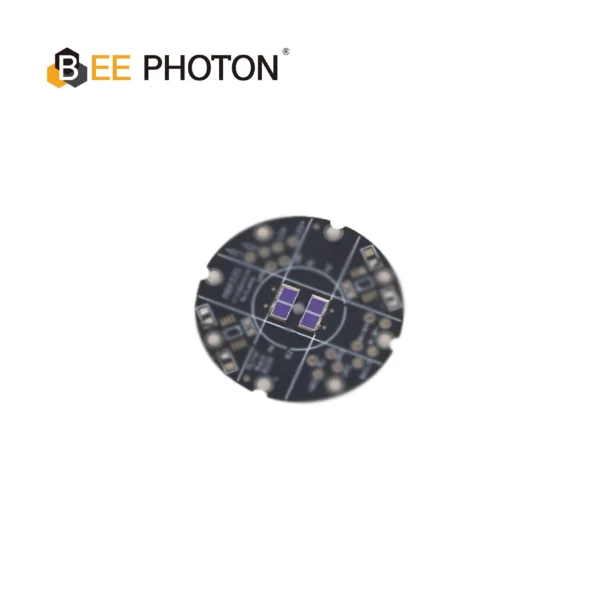
Si PIN photodiodes for Galvo PDC-C2929
The PDC-C2929 is a budget-friendly 920nm silicon PIN photodiode chip. This 920nm silicon PIN photodiode offers stable, cost-effective scanner position tracking.
How a Silicon PIN Photodiode Manufacturer Solves Space Constraints with COB Packaging
Space inside a modern laser galvo scanner is extremely tight. If you are packing driver boards, mirrors, motors, and sensing electronics into a tiny housing, every millimeter counts. This is why a top-tier silicon PIN photodiode manufacturer should always offer COB (Chip-on-Board) packaging solutions.
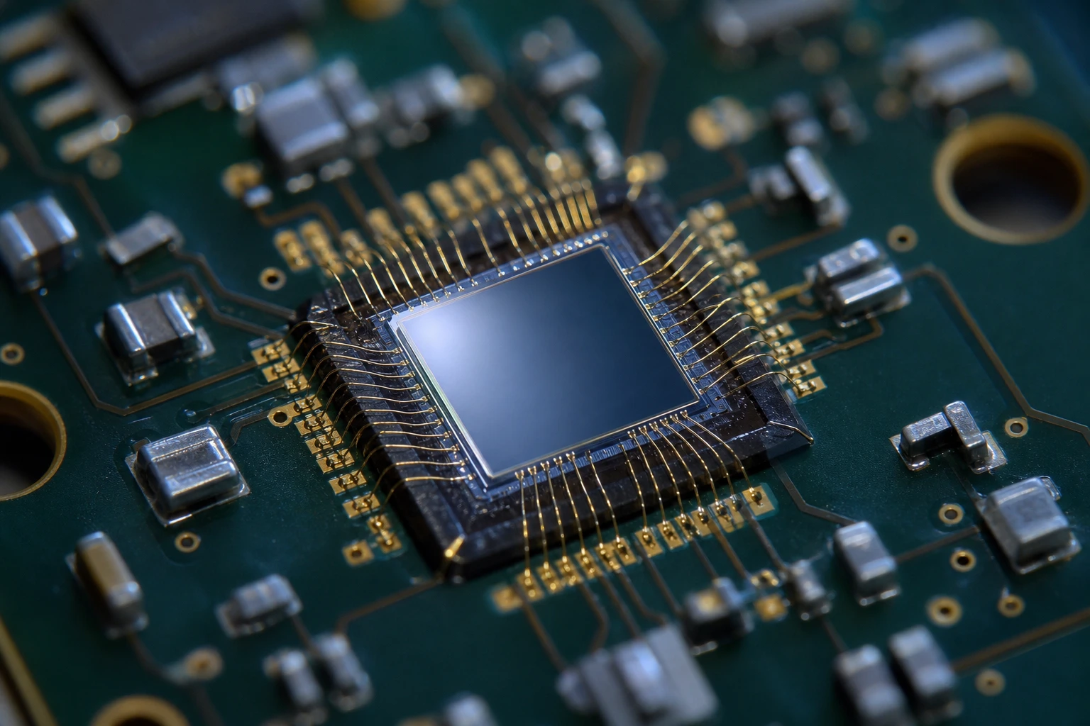
COB packaging eliminates the bulky ceramic or metal packages. Instead, the bare silicon photodiode die is bonded directly onto your custom PCB. A reliable silicon PIN photodiode manufacturer will handle the precise wire bonding and epoxy encapsulation at their own facility. This doesn’t just save space; it also radically improves electrical performance by minimizing parasitic inductance and capacitance.
Let’s look at the formula for photodiode bandwidth:
f_3dB = 1 / (2 * pi * RL * Cj)
Where f_3dB is the cutoff frequency, pi is approximately 3.14159, RL is the load resistance of your transimpedance amplifier (TIA), and Cj is the junction capacitance of the photodiode chip.
When a silicon PIN photodiode manufacturer uses COB packaging, the distance between the photodiode chip and your TIA is minimized. This reduces the stray capacitance that would otherwise add to Cj, allowing your scan head to achieve a much faster response time and sharper rise times.
The Role of a Silicon PIN Photodiode Manufacturer in Optimizing Responsivity and Speed
There is always a trade-off in photodiode design between speed and responsivity. If you make the active area larger to capture more light, the junction capacitance (Cj) increases, which slows down the response time. Junction capacitance is calculated as:
Cj = (epsilon_0 * epsilon_r * A) / d
Where epsilon_0 is the vacuum permittivity (8.854 * 10^-12 F/m), epsilon_r is the relative permittivity of silicon (about 11.7), A is the active area of the photodiode, and d is the width of the depletion region.
An experienced silicon PIN photodiode manufacturer can help you find the sweet spot. By modifying the depletion layer width (d) through advanced wafer fabrication techniques, a professional silicon PIN photodiode manufacturer can keep capacitance low even with a relatively large active area.
This is particularly important for high-performance laser marking where mirror movements happen in microseconds. You need a silicon PIN photodiode manufacturer who can provide chips optimized for fast rise times without losing sensitivity. For example, if you look at the Si PIN photodiodes for Galvo PDC-C2928-NIR-B, you get a chip designed specifically for 940nm NIR laser monitoring, where both responsivity and rise time are carefully balanced at the wafer level.
Evaluating Wafer-Level Capabilities of a Silicon PIN Photodiode Manufacturer
If you are a supply chain director, you probably know that many self-proclaimed manufacturers are actually just packaging houses. They buy silicon wafers from third-party foundries and package them in-house. While this works for generic applications, it represents a massive risk for high-reliability OEM/ODM projects. You should always choose a silicon PIN photodiode manufacturer that has direct wafer-level fabrication capabilities.
A true custom photodetector factory can control the starting material, the diffusion process, and the anti-reflective (AR) coating. For instance, different coatings can optimize the photodiode for different laser wavelengths. If your system uses a 920nm laser, a standard coating might reflect too much light. By choosing a dedicated silicon PIN photodiode manufacturer, you can specify a custom AR coating that minimizes reflection at 920nm, maximizing the light that actually enters the active region.
Take a look at the Si PIN photodiodes for Galvo PDC-C2929, which is a prime example of a wafer-optimized chip. A professional silicon PIN photodiode manufacturer designs these with specific doping profiles to handle the precise monitoring requirements of 920nm galvo scanners. This level of customization is simply impossible to get from standard distributors or packaging-only vendors.
Is Your Silicon PIN Photodiode Manufacturer a Direct Factory or a Middleman?
It can be surprisingly hard to tell the difference sometimes. Many brokers use clever marketing to look like they own the foundry. However, when you ask for specific custom modifications, they will suddenly become slow to respond, or they will quote outrageous minimum order quantities (MOQs). A genuine silicon PIN photodiode manufacturer will have no problem hopping on a technical call with your engineering team to discuss doping concentrations, guard rings, and wafer sorting.
Furthermore, working with a direct silicon PIN photodiode manufacturer like BeePhoton eliminates the middleman markup. If you are ordering in bulk, sourcing directly from a photodiode chip wholesale supplier guarantees that you get the best possible per-unit pricing. It also ensures that you receive detailed wafer testing reports, showing the distribution of dark current and responsivity across the entire batch.
Let’s be honest, in B2B procurement, consistency is everything. If your silicon PIN photodiode manufacturer changes their wafer source halfway through your product lifecycle, your system calibration will drift, leading to field failures and frustrated clients. Choosing a direct, vertically integrated supplier avoids this nightmare entirely.
Custom Laser Path Alignment: Collaboration with a Silicon PIN Photodiode Manufacturer
Laser path alignment in multi-axis galvo scan heads is notoriously difficult. A tiny mechanical vibration or temperature shift can throw the beam out of alignment. To solve this, many high-end systems use segmented photodiodes. These sensors feature multiple active areas separated by a very thin gap, known as the transition region.
By measuring the difference in photocurrent between the segments, your control system can calculate exactly where the laser beam is hitting. For a dual-segment photodiode, the position (X) of the beam can be approximated by:
X = (IA – IB) / (IA + IB)
Where IA and IB are the currents generated by segment A and segment B, respectively.
To make this work flawlessly, the gap between the segments must be extremely narrow and uniform. A standard supplier cannot achieve the sub-micron tolerances required for this. You need to partner with a high-precision silicon PIN photodiode manufacturer who can etch these patterns directly into the silicon wafer.
For example, the Si PIN photodiodes for Galvo PDC-2C3432-NIR-B is a specialized dual-segment chip designed specifically for high-accuracy galvo tracking. By working closely with an experienced silicon PIN photodiode manufacturer, you can customize the spacing and shape of these segments to match your system’s optical magnification and dynamic range.
When you buy from a reliable custom photodetector factory, you are not just buying a piece of silicon; you are buying engineering expertise. The engineers at your chosen silicon PIN photodiode manufacturer will help you model the beam profile and calculate the expected signal-to-noise ratio before they ever start cutting wafers. This collaborative approach saves months of trial-and-error during the prototyping phase.
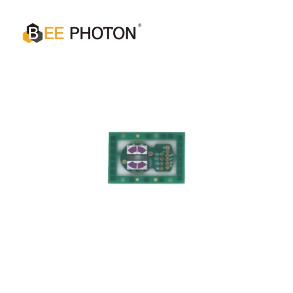
Si PIN photodiodes for Galvo PDC-2C3432-NIR-B
The PDC-2C3432-NIR-B is a specialized segmented PIN photodiode chip engineered for precise differential position feedback in high-speed galvanometer scanners. Integrating this dual-channel segmented PIN photodiode chip allows systems to obtain accurate angular tracking with minimal signal noise.
Mitigating B2B Supply Chain Risks with a Silicon PIN Photodiode Manufacturer
Over the past few years, supply chain resilience has become a top priority for procurement managers and supply chain directors. If your product relies on a single-sourced, off-the-shelf component from a large multi-national semiconductor company, you are at their mercy. If they decide to discontinue that part because the volume is too low compared to consumer electronics, your entire product line could go dark.
This is where a boutique, high-capability silicon PIN photodiode manufacturer becomes a vital strategic asset. A custom-focused manufacturer like BeePhoton doesn’t treat lower-volume B2B orders as an afterthought. They specialize in long-term supply agreements and can guarantee wafer availability for ten years or more.
By establishing a direct relationship with your silicon PIN photodiode manufacturer, you can arrange for buffer stock of finished chips or even raw wafers. If your sales suddenly spike, your silicon PIN photodiode manufacturer can quickly package and test additional parts from your dedicated wafer inventory, slashing lead times from months to weeks.
Additionally, a reliable B2B partner will offer transparent pricing. When dealing with a photodiode chip wholesale supplier, you can secure fixed pricing agreements that shield your margins from the volatile shifts of the general semiconductor market. This financial predictability is just as important as technical performance when you are trying to scale a complex optical scan head product line.
Quality Assurance Audits for Your Silicon PIN Photodiode Manufacturer
Before you sign a long-term supply agreement, you must thoroughly audit your potential silicon PIN photodiode manufacturer. A flashy website is nice, but you need to make sure they have the physical infrastructure to back up their claims.
Here is a quick checklist of what to ask your silicon PIN photodiode manufacturer during an audit:
- What cleanroom class do they use for wafer fabrication and COB packaging? (Class 100/ISO 5 or better is ideal for wire bonding).
- Do they perform 100% electro-optical testing at the wafer level, or do they just do sample testing?
- How do they track batches? Can they trace a specific BEE PHOTON photodiode back to the exact silicon ingot?
- What is their process for handling product change notifications (PCN)?
A professional silicon PIN photodiode manufacturer will welcome these questions. They will gladly share their ISO 9001 certifications and show you their testing setups. If a supplier hesitates or gives vague answers, that’s a massive red flag. Move on and find a partner who values transparency as much as you do.
Custom Silicon PIN Photodiode Comparison
To help you understand the diverse options available when working with a direct custom photodetector factory, let’s compare some common custom silicon PIN photodiode chips utilized in modern high-performance galvo systems.
| Product Model | Target Wavelength | Primary Application | Key Design Feature |
|---|---|---|---|
| PDC-C2928-NIR-B | 940 nm | NIR Laser Power Monitoring | High-responsivity chip designed for Si PIN photodiodes for Galvo PDC-C2928-NIR-B integration. |
| PDC-C2929 | 920 nm | Scan Head Optical Feedback | Custom doping profile optimized for Si PIN photodiodes for Galvo PDC-C2929 structures. |
| PDC-2C3432-NIR-B | 940 nm / Custom | Dual-Segment Beam Positioning | Ultra-narrow gap between active areas for Si PIN photodiodes for Galvo PDC-2C3432-NIR-B tracking. |
Real-World Case: Upgrading a Galvo Laser Marking System
Let’s look at an anonymous, real-world case study. A European manufacturer of ultra-compact metal 3D printers was struggling with thermal drift in their optical alignment system. They were using a standard catalog TO-can photodetector sourced from a massive distributor. Because the detector was packaged in a bulky metal can, it had to be placed far from the main sensor board, connected via long, noisy wires.
As the scan head warmed up during long printing runs, the dark current in the photodetector increased exponentially. For silicon, dark current (Id) roughly doubles for every 10 degrees Celsius rise:
Id(T) = Id(T0) * 2^((T – T0) / 10)
This rising dark current was misidentified by their system as actual laser signal, causing severe calibration drift and ruining expensive metal prints.
The company decided to bypass the distributor and partner directly with a specialized silicon PIN photodiode manufacturer. The engineering team at the custom photodetector factory analyzed their thermal profile and suggested two critical design changes:
- They switched to a custom COB package, mounting the bare silicon chip directly onto the TIA board. This eliminated the noisy wire runs and reduced the total assembly footprint by 65%.
- The silicon PIN photodiode manufacturer applied a specialized guard-ring structure on the silicon wafer itself. This modified the electric field distribution, drastically reducing the baseline dark current and making the sensor far less sensitive to operating temperature fluctuations.
The result? The thermal drift was virtually eliminated, and the 3D printer manufacturer slashed their assembly time by 40% because they no longer had to manually align the bulky TO-can packages. That is the power of working directly with a factory-level silicon PIN photodiode manufacturer.
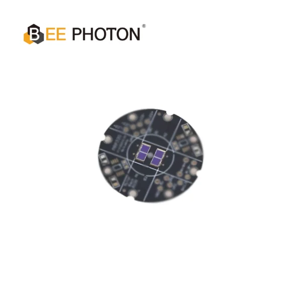
Si PIN photodiodes for Galvo PDC-C2928-NIR-B
Optimize scanning with our 940nm PIN photodiode chip, PDC-C2928-NIR-B. This 940nm PIN photodiode chip ensures precise galvo position sensing and low noise.
Frequently Asked Questions
Why should I choose custom COB packaging over standard TO-can packages for scan heads?
COB (Chip-on-Board) packaging allows the bare silicon die to be bonded directly onto your system’s PCB. This eliminates bulky housings, reduces parasitic capacitance, and improves response times. If you have tight spatial limitations in your scan head, a silicon PIN photodiode manufacturer can customize the COB layout to fit your exact dimensions, which is impossible with standard TO-cans.
How does a silicon PIN photodiode manufacturer control dark current in high-temperature environments?
A qualified silicon PIN photodiode manufacturer controls dark current at the wafer fabrication stage. They do this by optimizing the silicon substrate purity, using specialized diffusion profiles, and implementing guard rings. These features collect leakage currents before they can interfere with your primary signal, ensuring stable performance even as temperature rises.
What is the typical lead time and MOQ when working with a custom photodetector factory?
Because custom designs involve modifying the silicon wafer mask or wire-bonding setups, lead times can range from 6 to 12 weeks for prototypes. However, because a professional silicon PIN photodiode manufacturer owns the fabrication facility, they can often support highly flexible minimum order quantities (MOQs) for specialized industrial B2B programs, unlike larger consumer-focused semiconductor giants.
Can BeePhoton customize the spectral response of a photodiode chip for non-standard NIR wavelengths?
Yes. As a dedicated custom photodetector factory, BeePhoton can tune the spectral responsivity of the photodiode chip by adjusting the depth of the PIN junction and depositing custom anti-reflective (AR) coatings. This ensures peak quantum efficiency at precise wavelengths, such as 920nm or 940nm, tailored to your scanning system’s optical laser source.
Ready to Optimize Your Scan Head Performance?
If you are tired of dealing with bulky, catalog-standard detectors that force you to compromise your scan head design, it is time to upgrade your supply chain. Partnering with a dedicated, wafer-level silicon PIN photodiode manufacturer gives you the precise control over size, speed, and wavelength sensitivity that your application demands.
At BeePhoton, we help B2B procurement managers and optical engineers design, prototype, and manufacture custom photodetectors that fit their exact specifications. Whether you need specialized Si PIN photodiodes for Galvo PDC-C2928-NIR-B, custom Si PIN photodiodes for Galvo PDC-C2929 units, or high-accuracy Si PIN photodiodes for Galvo PDC-2C3432-NIR-B tracking chips, we have the engineering depth to deliver.
Stop dealing with distributors who don’t understand your technical challenges. Contact our engineering and sales team today to discuss your wafer-level customization requirements, request a custom quote, or obtain prototype samples.
- Email Us directly: info@photo-detector.com
- Visit our Contact Page: Get in touch with BeePhoton