If you’ve ever found yourself staring at a datasheet wondering whether to pick a 1 mm² or 10 mm² photodiode, you’re not alone. The photosensitive area size is one of those sneaky parameters that quietly controls almost everything else in your sensor’s behavior.
After spending the last twelve years helping clients pick the right photodiodes for everything from laser alignment systems to medical analyzers, I can tell you this: size really does matter — but not always in the way you think.
Let’s talk about what actually happens when you make the active area bigger (or smaller).
The Direct Relationship Between Photosensitive Area and Key Performance Metrics
The most obvious effect is on light collection. Double the photosensitive area size, and you roughly double the photocurrent for the same light intensity. Sounds great, right?
Not so fast.
Here’s what actually changes:
- Capacitance increases almost linearly with area
- Dark current scales with area
- Response speed usually drops
- Cost climbs (sometimes dramatically)
I’ve put together a quick comparison table based on real Si PIN photodiodes we commonly recommend:
| Active Area (mm²) | Typical Capacitance (pF) | Rise Time (ns) @ 10V | Dark Current (nA) | Relative Price |
|---|---|---|---|---|
| 1.0 (1×1mm) | 3 | 8 | 0.05 | 1.0x |
| 7.8 (2.8×2.8mm) | 20 | 25 | 0.4 | 1.8x |
| 13 (3.6×3.6mm) | 35 | 45 | 0.8 | 2.7x |
| 100 (10×10mm) | 250 | 280 | 6.5 | 9.5x |
Data compiled from BeePhoton’s Si PIN photodiode series measured at 10V reverse bias and 850nm.
You can see the trade-off is pretty brutal.
Why Junction Capacitance Explodes with Larger Photosensitive Area Size
This is the part most engineers feel in their circuits.
The junction capacitance ( C_j ) of a photodiode is approximately:
Cj ≈ ε × A / W
Where:
- ε is the permittivity of silicon
- A is the photosensitive area
- W is the depletion width
So when you increase the active area, capacitance goes up almost proportionally unless you dramatically increase the reverse voltage to widen the depletion region.
Why does this matter?
Because the RC time constant formed with your amplifier’s feedback resistor or the cable capacitance directly limits bandwidth. I’ve seen many projects fail because someone picked a large-area photodiode thinking “more light = better signal,” only to discover their bandwidth was trashed by 200pF of capacitance.
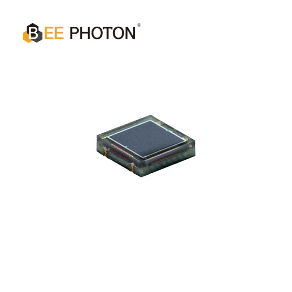
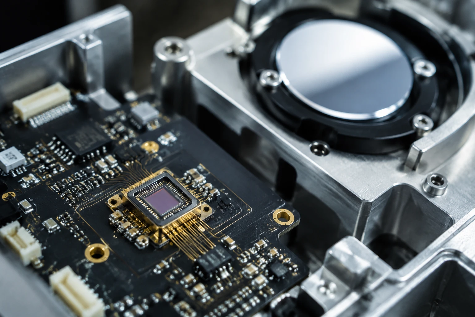
Si PIN Photodiode with NIR sensitivity enchanced (350-1100nm) PDCC34-501
Bee Photon offers a High Stability PIN Photodiode for precise industrial sensing. This NIR enhanced photodiode ensures reliable measurements from 350-1100nm. A top choice for a high stability photodiode.
Speed vs. Photosensitive Area Size: The Real Story
A lot of marketing material says “larger area = slower response.” That’s only half true.
What actually happens is the rise time has two main components:
- Transit time (time for carriers to cross the depletion region)
- RC-limited time (caused by capacitance)
For small photosensitive area size (< 4 mm²), transit time usually dominates. For larger detectors, RC effects take over.
In one industrial laser triangulation project we worked on, switching from a 5.8 mm² to a 1.2 mm² photodiode improved the system bandwidth from 8 MHz to over 35 MHz — even though the smaller diode collected less light. The improved SNR at high frequency more than compensated for the lower photocurrent.
Noise Performance and Large Area Photodiodes
This is where things get interesting.
Shot noise from dark current increases with the square root of area. But thermal (Johnson) noise is usually dominated by the feedback resistor, not the diode itself.
However, there’s another sneaky effect: as photosensitive area size grows, so does the chance of defects in the silicon. More defects = higher 1/f noise and higher leakage current variation across temperature.
I’ve seen some “large area photodiodes” that looked perfect at room temperature but became unusable above 50°C because dark current doubled every 8–10°C instead of the usual 10°C.
How to Choose the Right Photosensitive Area Size for Your Application
Here’s the practical framework I use with clients:
Choose small active area (≤ 4 mm²) when you need:
- High bandwidth (> 10 MHz)
- Low noise in high-frequency applications
- Tight cost control
- You can focus or collimate your light source
Choose larger photosensitive area size (> 9 mm²) when:
- Light is diffuse or scattered
- Alignment is difficult or unstable
- You’re working at very low light levels and speed isn’t critical
- You need maximum signal in DC or low-frequency measurements
For example, in fluorescence detection systems, we often recommend our large area photodiode options (typically 10–25 mm²) because the emitted light is weak and spreads out. But in LiDAR or optical communication, we push clients toward the smallest detector they can possibly use.
Real-World Trade-off Examples from the Field
Last year a medical device company came to us trying to detect very weak optical signals through tissue. Their first instinct was to use the biggest photodiode available. After testing, we actually went with a 2.9 × 2.9 mm active area Si PIN photodiode from our standard series.
Why?
Because the combination of lower capacitance and lower dark current allowed us to use higher gain in the transimpedance amplifier without hitting bandwidth or noise limits. The final system achieved 6 dB better SNR than the “bigger is better” approach.
Another client in industrial automation needed to detect a laser spot over a 15-meter distance with ±0.5 mm accuracy. Everyone expected we’d need a large area photodiode. Instead, we used a small 1 mm² quadrant detector with excellent optics. The smaller photosensitive area size gave us much faster response and better position resolution.

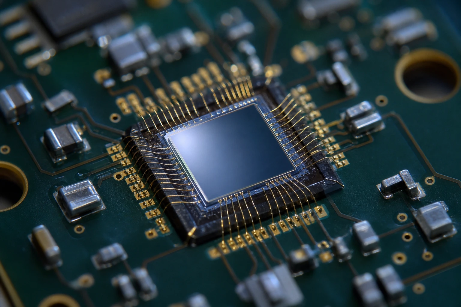
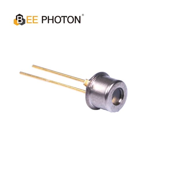
Si PIN Photodiode with low dark current (350-1060nm) PDCC100-001
Looking for a custom Si PIN photodiode? Bee Photon provides OEM solutions with low dark current and a 350-1060nm range. We partner with B2B clients to develop photodiodes tailored to your specific needs.
Understanding the Cost Implications
Let’s be honest — bigger isn’t just electrically different, it’s financially different too.
Silicon real estate is expensive. A 10 × 10 mm photodiode doesn’t just cost more because of the package — the yield drops significantly as the active area grows due to defects.
That’s why you’ll often see price jumping sharply above 5–7 mm².
Our Si PIN photodiodes reflect this reality. The jump from 2.9×2.9mm to 5.8×5.8mm typically doubles the unit price in volume.
Practical Tips for Working with Different Photosensitive Area Sizes
If you’re designing with larger area detectors:
- Consider using a bootstrap amplifier or current amplifier instead of traditional TIA to reduce the effect of capacitance
- Pay serious attention to stray capacitance in your PCB layout
- Consider using higher reverse bias (if your diode can handle it) to reduce capacitance
- Don’t forget temperature effects — they get worse with larger areas
For smaller detectors, your main challenge is usually collecting enough light. Here good optics and proper alignment become critical.
Making the Right Choice for Your Next Project
At the end of the day, there’s no universal “best” photosensitive area size. There’s only the best size for your specific requirements, budget, and constraints.
The key is understanding the real trade-offs instead of just picking the biggest detector that fits in your package.
If you’re currently wrestling with this decision, I’d be happy to look at your requirements. Drop us a message on our contact page or shoot an email to info@photo-detector.com. We’ve helped dozens of companies navigate exactly these choices, and we’re pretty good at finding the sweet spot between performance and cost.
Si PIN Photodiode with low dark current (350-1060nm) PDCT01-201
Experience superior signal clarity with our Si PIN photodiode, engineered for ultra-low dark current and high stability. This photodiode ensures precise laser detection and optical measurements. Our low dark current Si PIN photodiode offers exceptional performance.
FAQ
Does a larger photosensitive area size always mean better sensitivity?
No. While a larger active area collects more photons, the accompanying increase in capacitance and dark current often degrades overall signal-to-noise ratio, especially at higher frequencies. Sometimes a smaller, better-optimized detector performs better.
How does photosensitive area size affect response time?
Larger area photodiodes have significantly higher junction capacitance, which increases the RC time constant and slows response. The effect becomes particularly noticeable above 5–7 mm².
Is it worth paying more for a large area photodiode?
Only if your application actually needs it. If you can concentrate your light onto a smaller active area through optics, you’ll usually get better speed, lower noise, and lower cost by choosing a smaller photosensitive area size.
Ready to find the perfect balance for your sensor design?
Head over to our Si PIN photodiodes collection or contact us directly. We’ll help you pick the right active area without the usual headaches.