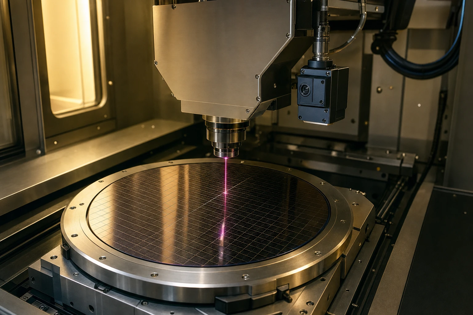
If you are an optical R&D engineer designing galvo-based industrial laser scanners, you know how annoying the receiver end can be. You spend weeks perfecting the laser source, the mirrors, the scanning angles, only to realize the receiver is slow or deaf to the signals. Often, the culprit is choosing the wrong 940nm PIN photodiode chip. At 940nm, silicon’s light absorption starts to drop off quite a bit, making sensor selection a delicate balancing act.
Selecting a high-quality 940nm PIN photodiode chip isn’t just about picking a part from a datasheet; it’s about matching chip physics with real-world system limits. Whether you are working on LiDAR, B2B sorting systems, or high-speed rangefinders, selecting the right 940nm PIN photodiode chip can make or break your design. Let’s dive deep into what matters when picking a 940nm PIN photodiode chip for industrial laser scanning.
When you start sourcing a 940nm PIN photodiode chip, you’re looking for a balance between speed, sensitive area, and responsivity. If the active area of the 940nm PIN photodiode chip is too small, alignment becomes a nightmare. If the active area of the 940nm PIN photodiode chip is too big, the capacitance slows down your system. You cannot afford to make the wrong choice when designing high-speed industrial scanners. Let’s look at how to navigate these challenges.
Active Area vs. Speed: The Ultimate Trade-off in a 940nm PIN Photodiode Chip
Let’s get right into the physics. Why can’t we just use a massive active area for our 940nm PIN photodiode chip? It would make laser alignment so much easier, right? Yes, but your circuit would become painfully slow. When selecting a 940nm PIN photodiode chip, you’re constantly fighting junction capacitance.
The junction capacitance of a 940nm PIN photodiode chip acts like a low-pass filter in your receiver circuit. To keep things moving fast in a high-speed galvo scanner, you need that capacitance as low as possible. If your 940nm PIN photodiode chip has a high capacitance, your signal rise time increases, and you lose the sharp edges of your reflected laser pulses. This is a common issue when trying to use a generic 940nm PIN photodiode chip that wasn’t specifically optimized for high-speed laser detection.
For most industrial galvo systems, you want to look at a silicon PIN photodiode die that offers a moderate active area but uses special NIR enhancement to keep the depletion region thick. A thick depletion region lowers the capacitance while maximizing the absorption of 940nm photons. This means your 940nm PIN photodiode chip can remain highly responsive without turning into a slow, capacitive slug.
The Math Behind Junction Capacitance and Rise Time
Let’s look at the actual formulas you need to use during your design phase. Don’t worry, we won’t use complex LaTeX; we will keep it simple and easy to copy directly into your notes.
The classic formula for junction capacitance of a 940nm PIN photodiode chip is:
Junction Capacitance (Cj) = (Permittivity of Silicon * Active Area) / Depletion Width
Where:
- Permittivity of Silicon is approximately 1.04 * 10^-10 Farads per meter (F/m).
- Active Area is the actual light-sensitive area of the chip in square meters.
- Depletion Width is the thickness of the reverse-biased region in meters.
As you can see, if the active area of your 940nm PIN photodiode chip increases, the junction capacitance goes up proportionally. To combat this, you can apply a reverse bias voltage. When you apply a reverse bias to the 940nm PIN photodiode chip, the depletion width increases, which pulls the capacitance down.
Once you know your capacitance, you can estimate the rise time (tr) of your 940nm PIN photodiode chip using this formula:
Rise Time (tr) = 2.2 * Load Resistance * Total Capacitance
Where:
- Load Resistance is the feedback or input resistor of your pre-amplifier circuit (often a transimpedance amplifier).
- Total Capacitance is the sum of the junction capacitance of your 940nm PIN photodiode chip and any stray capacitance on your PCB layout.
If you are aiming for a rise time of under 10 nanoseconds to catch fast galvo reflections, you can quickly see why a massive 940nm PIN photodiode chip with high capacitance is out of the question unless you can tolerate very low transimpedance gains or high reverse bias voltages.
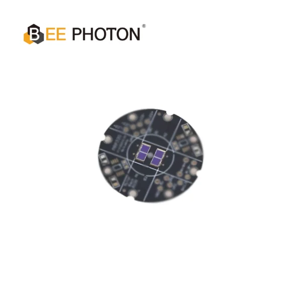
Si PIN photodiodes for Galvo PDC-C2928-NIR-B
Optimize scanning with our 940nm PIN photodiode chip, PDC-C2928-NIR-B. This 940nm PIN photodiode chip ensures precise galvo position sensing and low noise.
Why Silicon PIN Photodiode Die is Preferred Over Standard Silicon
When looking at options, you might wonder if a standard PN photodiode chip is good enough. Let’s be completely honest: for industrial laser scanning, it’s not. You need a 940nm PIN photodiode chip because of that intrinsic “I” layer between the P and N regions.
The intrinsic layer of a 940nm PIN photodiode chip allows for a much wider depletion region at lower reverse bias voltages. This wide depletion region is crucial for 940nm light. Why? Because 940nm is in the near-infrared (NIR) spectrum, and silicon has a relatively low absorption coefficient at this wavelength. 940nm photons need to travel deeper into the silicon before they are absorbed and converted into electron-hole pairs.
If you use a standard PN structure instead of a 940nm PIN photodiode chip, many of the 940nm photons will pass right through the active depletion region and generate carriers in the bulk substrate. These carriers have to diffuse slowly back to the junction, which creates a “diffusion tail” in your signal. This diffusion tail ruins the speed of your receiver, making your fast laser pulses look muddy and slow. A dedicated NIR photodetector chip with a PIN structure prevents this by ensuring that almost all carrier generation happens within the high-field depletion region, giving you a clean, crisp electrical response.
Aligning the Laser Spot on Your 940nm PIN Photodiode Chip
Let’s talk about the practical side of designing industrial galvo scanners. Galvo mirrors are fast, and they move the laser beam across a wide target area. The reflected light that returns to your receiver system is focused by a lens onto the sensitive surface of your 940nm PIN photodiode chip.
If your laser spot moves slightly due to optical aberrations, thermal drift, or mechanical vibration, a small active area on your 940nm PIN photodiode chip will cause signal loss. This is where many engineers get stuck. They choose a tiny 940nm PIN photodiode chip to get ultra-fast response times, only to find that their optical alignment window is so tight that the system fails during assembly or after a few hours of operation in a warm factory.
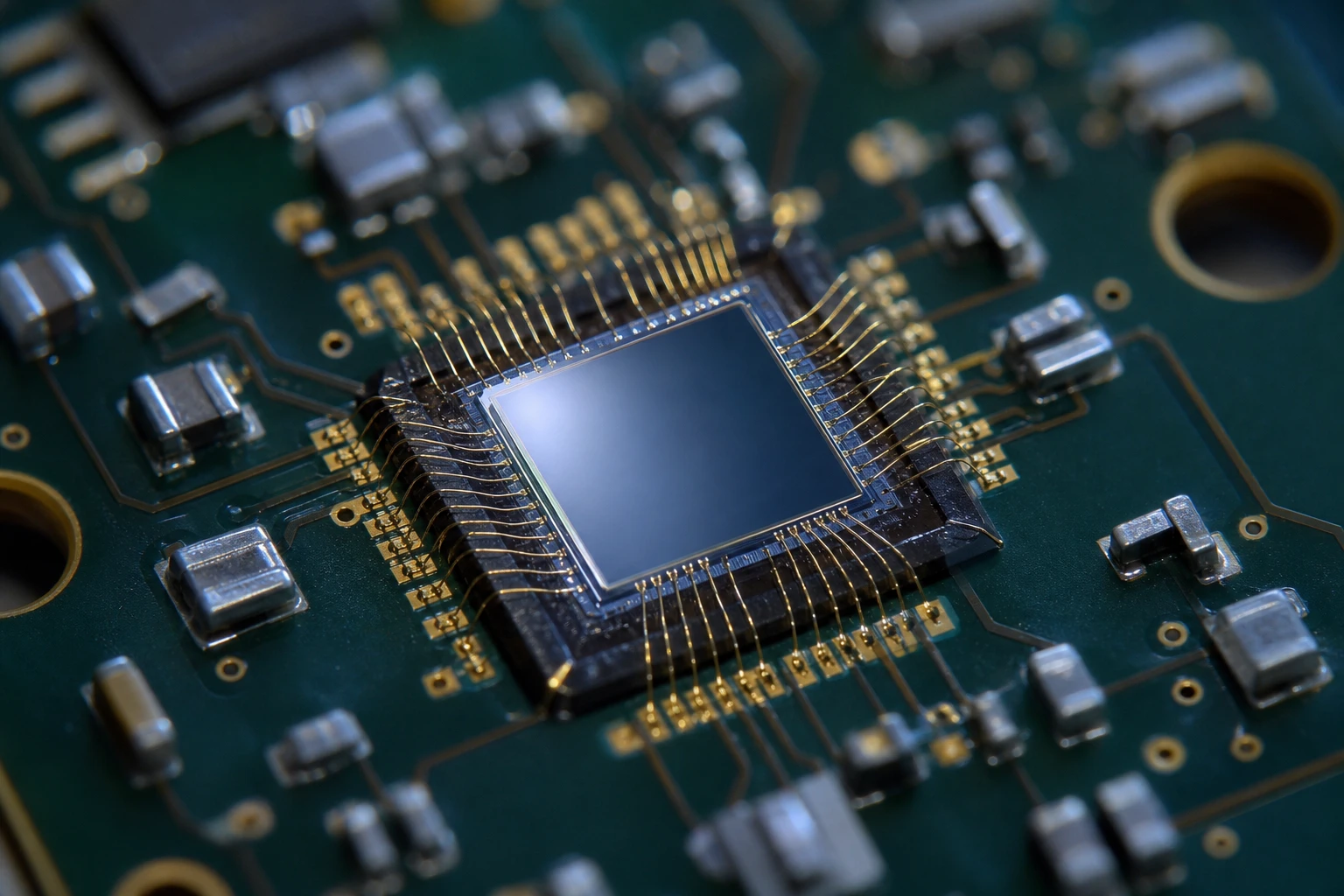
To solve this, you need a 940nm PIN photodiode chip that offers a medium-large active area but is designed with specialized high-speed silicon processing to keep capacitance low. This is exactly why the Si PIN photodiodes for Galvo PDC-C2928-NIR-B from BeePhoton are so popular. This specific 940nm PIN photodiode chip features an active area of 2.8 mm x 2.8 mm, which provides an excellent balance. It gives your optical designer plenty of breathing room for alignment, yet still keeps the junction capacitance low enough to handle fast scanning rates.
Understanding Responsivity and Quantum Efficiency at 940nm
When comparing a 940nm PIN photodiode chip from different suppliers, look closely at the responsivity curves. Responsivity (R) measures how much electrical current the 940nm PIN photodiode chip produces for a given amount of optical power. It’s usually expressed in Amperes per Watt (A/W).
At 940nm, the theoretical maximum responsivity for a silicon photodiode is around 0.75 A/W. However, standard silicon chips often drop to 0.4 A/W or lower at 940nm because the silicon wafer isn’t thick or optimized enough to catch those deep NIR photons. When selecting a 940nm PIN photodiode chip, make sure it has an NIR-enhanced design. An NIR-enhanced 940nm PIN photodiode chip can achieve a responsivity of 0.55 A/W to 0.60 A/W at 940nm, which represents a massive boost to your optical link budget.
You can calculate the quantum efficiency (QE) of your 940nm PIN photodiode chip using this straightforward formula:
Quantum Efficiency (%) = (Responsivity * 1240) / Wavelength in nanometers
If you have an NIR-enhanced 940nm PIN photodiode chip with a responsivity of 0.60 A/W at 940nm, let’s calculate its quantum efficiency:
QE = (0.60 * 1240) / 940 = 744 / 940 = 79.1%
That is a highly impressive efficiency for silicon at this wavelength. A standard, non-optimized silicon chip might only have a QE of 40% to 50% at 940nm, meaning you would need to blast more laser power to get the same signal. That raises your system cost, increases eye-safety concerns, and generates more heat. Choosing a highly efficient 940nm PIN photodiode chip is simply a much smarter way to design.
Specifications Comparison: Choosing the Right 940nm PIN Photodiode Chip
To help you visualize the difference between a generic chip and a specialized chip for industrial galvo scanning, let’s put the specs side-by-side in a table. Here is a comparison of a standard silicon PIN die, a tiny high-speed die, and the specialized Si PIN photodiodes for Galvo PDC-C2928-NIR-B from BeePhoton.
| Parameter | Standard Silicon PIN Die | Tiny High-Speed Die | PDC-C2928-NIR-B 940nm PIN photodiode chip |
|---|---|---|---|
| Active Area (mm) | 1.0 x 1.0 | 0.5 x 0.5 | 2.8 x 2.8 |
| Active Area Size (mm2) | 1.0 | 0.25 | 7.84 |
| Responsivity at 940nm (A/W) | 0.40 | 0.35 | 0.60 |
| Junction Capacitance (pF) | 15 (at 10V bias) | 3 (at 10V bias) | 22 (at 15V bias) |
| Rise Time (ns) | 15 | 1.5 | 8 |
| Optical Alignment Tolerance | Medium-Low | Extremely Low (Hard) | High (Very Easy) |
| Dark Current at 25C (nA) | 1.0 | 0.1 | 0.8 |
As the table shows, while the tiny die is incredibly fast, its tiny active area makes optical alignment practically impossible in high-vibration industrial galvo systems. On the other hand, the standard silicon PIN die has a decent size but lacks the NIR spectral sensitivty and speed you need. The PDC-C2928-NIR-B 940nm PIN photodiode chip gives you the best of both worlds: a large 2.8 x 2.8 mm active area, high responsivity at 940nm, and a fast 8 ns rise time when reverse biased at 15V. It is a highly specialized tool designed specifically for this job.
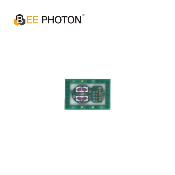
Si PIN photodiodes for Galvo PDC-2C3432-NIR-B
The PDC-2C3432-NIR-B is a specialized segmented PIN photodiode chip engineered for precise differential position feedback in high-speed galvanometer scanners. Integrating this dual-channel segmented PIN photodiode chip allows systems to obtain accurate angular tracking with minimal signal noise.
The Role of Dark Current and Noise in Weak Signal Detection
In industrial laser scanning, you aren’t always working with strong, clean laser reflections. If you are scanning dark, rough, or highly absorbent surfaces (like matte black plastics or wet metals), the reflected light returning to your 940nm PIN photodiode chip can be incredibly weak.
When dealing with weak signals, the noise floor of your 940nm PIN photodiode chip becomes the limiting factor. The primary source of noise in the chip itself is dark current. Dark current is the residual current that flows through the 940nm PIN photodiode chip even when there is absolutely no light hitting the sensor.
Dark current is highly temperature-dependent. As a general rule of thumb, dark current doubles for every 10 degrees Celsius increase in temperature. If your industrial scanner is mounted inside a hot factory floor near heavy machinery, your 940nm PIN photodiode chip will warm up, its dark current will rise, and your signal-to-noise ratio will degrade.
To minimize this issue, you must choose a 940nm PIN photodiode chip from a 940nm silicon detector OEM that uses high-purity silicon wafers and precise manufacturing steps to minimize surface leakage and crystal defects. A well-manufactured 940nm PIN photodiode chip like those from BeePhoton will keep dark current below 1 nA at room temperature, ensuring that your scanner can detect even the weakest reflections in hot, harsh environments.
Sourcing Challenges: Finding a Reliable 940nm Silicon Detector OEM
As an R&D engineer or B2B buyer, you don’t just care about the specs on a PDF datasheet. You also have to worry about long-term supply chain stability, chip-to-chip consistency, and ease of assembly. Sourcing a 940nm PIN photodiode chip can be a real headache if you choose the wrong supplier.
When you buy a raw 940nm PIN photodiode chip (often supplied as a bare silicon die), your assembly team must perform die bonding and wire bonding. If the metalization on the top anode and back cathode of the 940nm PIN photodiode chip isn’t highly consistent, your wire bonder will struggle. You’ll end up with weak wire bonds, lifted pads, and high field-failure rates.
Furthermore, you need a supplier that offers excellent wafer-level sorting. Silicon wafers naturally have performance variations between the chips in the center and those on the outer edges. A reliable 940nm silicon detector OEM like BeePhoton performs rigorous testing and binning to ensure that every single 940nm PIN photodiode chip you receive meets the exact same electrical and optical specifications. This level of consistency is critical for industrial applications where recalibrating every single scanner on the production line is too expensive.
Real-World Success: Redesigning a Sorting LiDAR Receiver
Let’s look at a quick, anonymous real-world example of how choosing the right 940nm PIN photodiode chip solved a massive production headache. A manufacturer of high-speed industrial sorting LiDAR systems was using a generic silicon PIN photodiode chip they sourced from an online catalog.
The system worked fine in their air-conditioned lab, but once it was deployed in a recycling facility, things went sideways. The sorting machines were subject to heavy vibrations and high temperatures. The tiny photodiode chips they used were constantly falling out of alignment due to mechanical drift, causing the sorting system to miss targets. When they tried to use a larger, standard photodiode chip, the response time dropped so much that the system could no longer resolve small objects at high belt speeds.
They reached out to BeePhoton for a custom evaluation of their optical receiver. After analyzing their setup, the engineering team recommended replacing their generic sensor with the PDC-C2928-NIR-B 940nm PIN photodiode chip. Thanks to its 2.8 mm x 2.8 mm active area, the alignment issues vanished overnight. The optical path could tolerate minor mechanical drift without losing signal.
Even better, because the PDC-C2928-NIR-B 940nm PIN photodiode chip was engineered for enhanced NIR responsivity and low capacitance, they didn’t have to sacrifice any speed. The system’s rise time stayed well within their 10 ns limit. By swapping to a high-quality, application-specific 940nm PIN photodiode chip, they reduced their manufacturing assembly time by 40% and completely eliminated field returns due to alignment drift.
Best Practices for Integrating a 940nm PIN Photodiode Chip onto Your PCB
Once you have selected your 940nm PIN photodiode chip, your job isn’t quite done. You still have to lay out your receiver board correctly. Since a 940nm PIN photodiode chip outputs tiny currents (often in the microampere or nanoampere range), your PCB layout is highly vulnerable to external electromagnetic interference (EMI) and parasitic noise.
Here are a few quick, practical tips for integrating your 940nm PIN photodiode chip:
- Keep the Pre-Amplifier Close: Place your transimpedance amplifier (TIA) as physically close to the 940nm PIN photodiode chip as possible. Every millimeter of trace between the photodiode anode and the TIA input acts like an antenna that picks up noise from your galvo motor drivers and switching power supplies.
- Use Guard Rings: Run an analog ground guard ring around the high-impedance input trace of your 940nm PIN photodiode chip. This helps intercept surface leakage currents flowing across the PCB substrate, especially in high-humidity environments.
- Decouple the Bias Voltage: If you are applying a reverse bias voltage to your 940nm PIN photodiode chip to speed it up, make sure that bias line is clean. Use a series resistor and a high-quality ceramic bypass capacitor to filter out any high-frequency ripple from your power supply.
- Shield the Entire Receiver: If your galvo scanner operates near high-power laser drivers or RF sources, place a metal shielding can over your 940nm PIN photodiode chip and its pre-amplifier stage.
By following these simple steps, you can ensure that the high performance of your specialized 940nm PIN photodiode chip isn’t wasted by a noisy board layout.
Si PIN photodiodes for Galvo PDC-C2929
The PDC-C2929 is a budget-friendly 920nm silicon PIN photodiode chip. This 920nm silicon PIN photodiode offers stable, cost-effective scanner position tracking.
FAQs About Using a 940nm PIN Photodiode Chip
1. Why should I choose 940nm over 850nm for my industrial laser scanner?
While silicon photodiodes naturally have higher responsivity at 850nm, 940nm is often preferred because of ambient sunlight interference. Sunlight has a strong absorption band in the atmosphere around 940nm, meaning there is less background ambient solar noise at this wavelength. If your industrial scanner has to work near windows, outdoors, or in highly lit factory environments, using a 940nm PIN photodiode chip paired with a 940nm bandpass filter will give you a much higher signal-to-noise ratio than an 850nm system.
2. What reverse bias voltage should I apply to my 940nm PIN photodiode chip?
This depends on your speed requirements. Applying a higher reverse bias (such as 10V to 15V) widens the depletion layer, which drops the capacitance and speeds up your 940nm PIN photodiode chip. However, a higher bias also increases dark current and heat dissipation. For most galvo scanning applications, a reverse bias between 5V and 15V strikes the perfect balance between low capacitance and low dark current.
3. Can I use a 940nm PIN photodiode chip as a bare die, or do I need a package?
You can use it as a bare silicon PIN photodiode die if you have die-bonding and wire-bonding capabilities in-house or through a packaging partner. Bare die mounting is ideal for space-constrained designs and optical systems where you want to minimize any glass or epoxy interfaces. However, if you want easier assembly, you can ask a 940nm silicon detector OEM like BeePhoton to supply the chip in a standard SMD or TO-can package with a built-in daylight filter window.
4. What is the difference between gold and aluminum wire bonding for a bare 940nm PIN photodiode chip?
Gold ball bonding is faster and highly reliable, but it requires heating the substrate (usually to around 150 degrees Celsius). Aluminum wedge bonding can be done at room temperature, which is gentler on some sensitive optical substrates. Make sure to specify your preferred wire bonding pad metallization when ordering your 940nm PIN photodiode chip from your manufacturer so they can supply the correct top-contact metal finish.
Take Your Optical Receiver Design to the Next Level
If you are tired of dealing with slow response times, alignment headaches, and inconsistent chip quality, it’s time to upgrade your receiver stage. Designing a high-performance galvo laser scanner requires a 940nm PIN photodiode chip that is built for the job, not a cheap generic part from an online catalog.
By partnering with a specialized manufacturer like BeePhoton, you get access to world-class optoelectronic engineering support and highly consistent, premium-grade silicon chips. Whether you need bare dies for direct integration or packaged sensors with custom bandpass filters, we have the manufacturing flexibility and engineering expertise to deliver exactly what your project demands.
Don’t let a sub-par detector hold back your laser scanning hardware. Browse our full selection of high-speed silicon detectors, including the specialized Si PIN photodiodes for Galvo PDC-C2928-NIR-B.
If you have a unique mechanical layout or a challenging optical budget, reach out to our engineering team directly through our contact page or drop us a line at info@photo-detector.com. We can provide custom wafer-level dicing, custom metallization, and detailed test reports to help you get your project done right the first time. Let us help you build a faster, more reliable industrial scanner today.