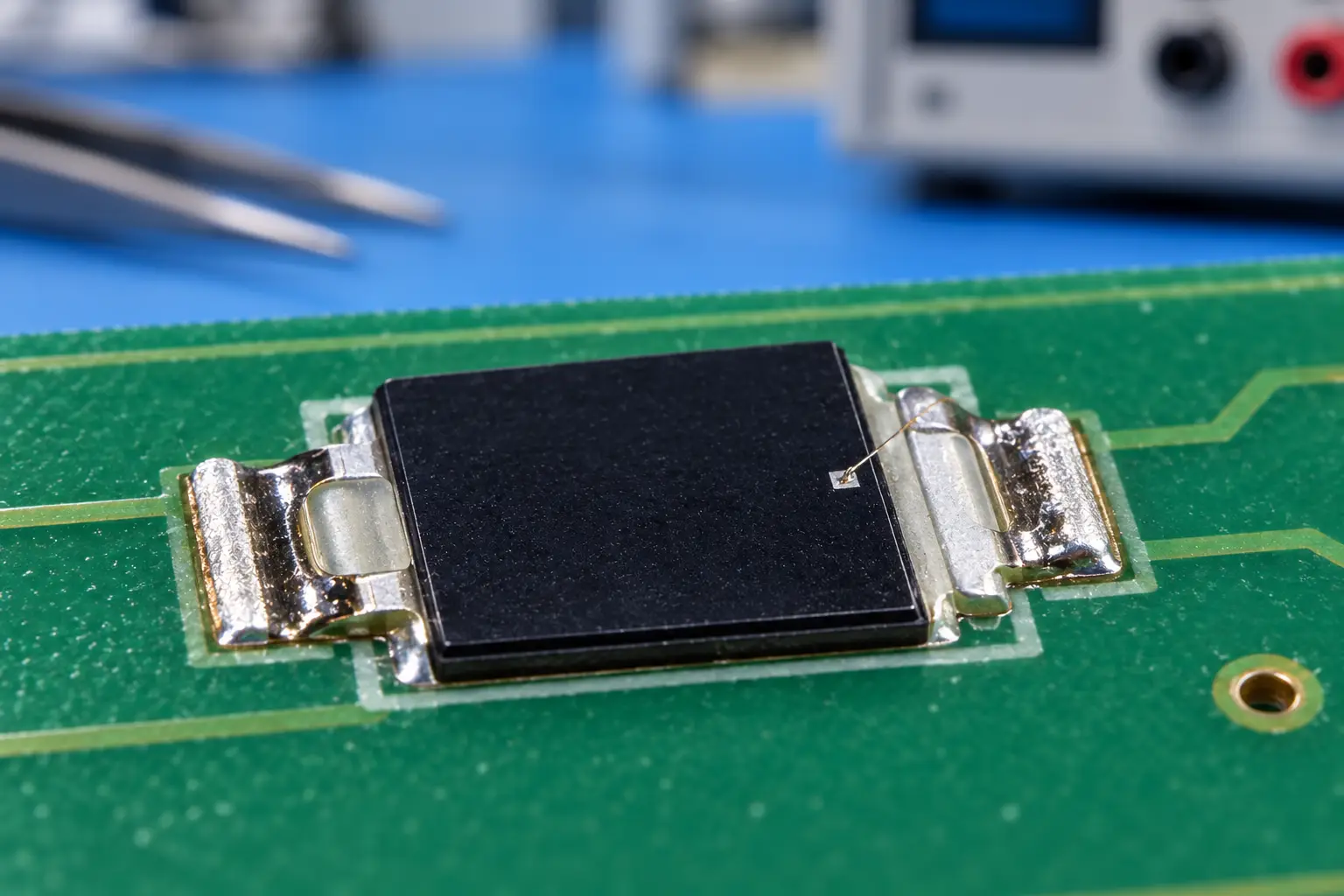
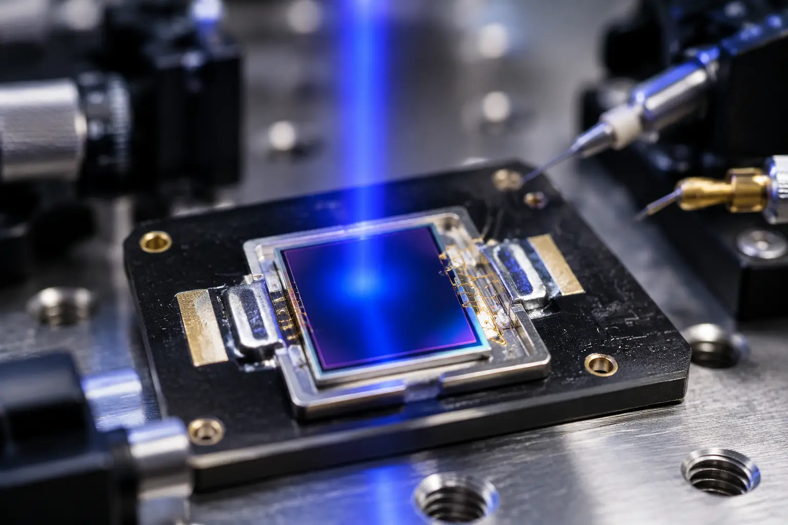
Most hardware engineers have had this exact headache on the test bench. You pick a high-output 850nm LED from one vendor, grab a silicon detector from another, lay them out on a board, and fire up your prototype. On paper, the emitter kicks out plenty of milliwatts, and the detector has decent responsivity. Yet in testing, you either run straight into transimpedance amplifier saturation at close range or watch your signal sink into the noise floor once the sensor moves ten centimeters away.
Treating the emitter and receiver as isolated catalog items is the quickest way to botch an optical sensing link. An efficient optoelectronic setup always functions as a coupled system. Whether you are building an industrial light curtain, an automated liquid level detector, an optical tachometer, or a short-range proximity gate, selecting a matched IR photodiode emitter pair saves weeks of circuit redesign and layout revisions.
Optimizing an IR photodiode emitter pair involves more than matching nominal peak wavelengths. You have to account for spatial emission profiles, detector active area dimensions, ambient daylight leakage, package thermal drift, and amplifier bandwidth.
1. The Core Physics of an IR Photodiode Emitter Pair Link
To get reliable data from an IR photodiode emitter pair, skip the vendor sales pitches and look straight at the transfer function. Your detector generates a photocurrent based on the fraction of emitted radiant flux that actually lands on its active silicon area.
System Optical Path Flow:
IR LED Emitter (Radiant Intensity: I(θ))
➔ Spatial Propagation Path (Distance d, Emission Angle θ, Incidence Angle φ)
➔ Silicon Photodiode Sensor (Detector Active Area: A_det)
➔ Output Photocurrent Generation (Signal: I_ph)
The generated photocurrent is governed by detector responsivity:
I_ph = P_rx * R(λ)
Where:
- I_ph is the generated signal photocurrent in amperes.
- P_rx is the optical power hitting the detector active area in watts.
- R(λ) is the spectral responsivity of the photodiode in amperes per watt (A/W) at the specific operating wavelength λ.
According to fundamental radiometric standards maintained by institutions like the National Institute of Standards and Technology, measuring radiant intensity requires evaluating angular flux distribution rather than relying solely on raw electrical input wattage.
Calculating Incident Optical Power on the Detector
Most clear-molded and lensed infrared emitters exhibit a radiant intensity profile approximated by Lambert’s cosine law:
I(θ) = I_0 * cos^m(θ)
Where I_0 is the on-axis radiant intensity (measured in mW/sr), θ is the emission angle relative to the optical mechanical axis, and m is an exponent determined by the package lensing geometry. A bulbous dome lens yields a higher value of m (narrowing the beam), whereas a flat-window surface-mount LED yields m approximately equal to 1.
The radiant flux arriving at your detector face over a separation distance d is calculated as:
P_rx = [ I(θ) / d^2 ] * A_det * cos(φ) * η_opt
Where:
- d is the distance separating the emitter lens from the detector window.
- A_det is the active area of the receiving photodiode die (mm²).
- φ is the incidence angle of the light beam hitting the photodiode surface normal.
- η_opt accounts for transmission losses through external optical filters, protective acrylic windows, or internal dust barriers.
If you mismatch your IR photodiode emitter pair by pointing an ultra-wide LED at a microscopic photodiode die across a 150mm gap, your geometric coupling efficiency drops below 0.05%. You end up compensating by pumping excessive forward current through the LED, driving up component temperature and accelerating LED lumen depreciation.
2. Emission Angles vs. Photodiode Active Area: 4°, 20°, or 120°?
Beam shape is where many custom optical links fall apart. When sourcing a matched IR photodiode emitter pair, beam angle must pair directly with the active sensor die size and mechanical tolerances of your housing.
Spatial Beam Profiles at a Glance:
- Narrow Beam (4° to 8°): Concentrated parallel beam for long-range links requiring strict mechanical alignment.
- Medium Beam (20° to 35°): Focused conical emission providing a balanced trade-off between range and angular tolerance.
- Wide Angle (120° Lambertian): Hemispherical flood pattern designed for short-range diffuse sensing and reflection detection.
| Emission Angle (2θ 1/2) | Optical Coupling Character | Best Suited Detector Type | Typical Range | Main Engineering Risk |
|---|---|---|---|---|
| 4° to 8° (Narrow) | Extremely high on-axis mW/sr, concentrated optical flux | Small active area (0.5 to 1.5 mm²), fast PIN photodiode | 500mm to 5000mm | Severe axis misalignment failure from mechanical vibration |
| 20° to 35° (Medium) | Balanced energy density, generous alignment margin | Medium active area (3.0 to 7.5 mm²), standard planar PIN photodiode | 50mm to 500mm | Partial beam clipping on custom enclosure apertures |
| 120° (Wide Lambertian) | Broad spatial flood pattern, rapid inverse-square power drop | Large active area (7.5 mm² and up), high-capacitance photodiode | 1mm to 50mm | Low SNR, internal optical crosstalk inside device housing |
The 4° to 8° Narrow-Angle Emitter Configuration
A 4° to 8° emitter uses an integrated collimating or deep parabolic lens to project an intense beam along its mechanical axis.
- The Advantage: On-axis intensity spikes dramatically. A standard 20mA drive current can easily deliver over 100 mW/sr of radiant intensity.
- The Drawback: Mechanical tolerance stack-up will punish you. If your assembly workers mount the emitter tilted just 2 degrees off-axis on the PCB, your optical flux misses the photodiode die entirely at 30 centimeters.
- Matched Receiver Strategy: Pair narrow-angle emitters with high-speed PIN photodiodes featuring compact active areas. A smaller silicon chip keeps junction capacitance low and edge-transition speeds crisp. Precision-tooled mechanical locating pins or custom optical alignment brackets are non-negotiable here.
The 20° to 35° Medium-Angle Setup
This profile is the workhorse for industrial factory automation, edge detection, and safety barriers.
- The Balance: It balances comfortable assembly tolerances with enough energy density to cover working distances between 50mm and 500mm.
- Matched Receiver Strategy: For an all-around IR photodiode emitter pair, team a 20° emitter with a surface-mount detector like the PDCP08-502 silicon PIN photodiode. Its 2.9×2.8mm footprint provides an optimal collection area without introducing the sluggish capacitive response typical of oversized silicon wafers.
The 120° Wide-Angle (Lambertian) Setup
Wide-angle emitters lack secondary internal lenses. Light spreads in a broad cone across the board surface.
- Primary Applications: Reflective proximity sensors, paper-feed detection, short-throw optical switches, and diffuse code readers.
- The Drawback: Optical energy decays rapidly over distance. Because flux spreads across a hemisphere, stray light bounces off interior enclosures, often triggering false positives.
- Matched Receiver Strategy: Pair wide emitters with large-area receivers, such as the PDCP08-501 silicon PIN photodiode. Its broad silicon surface captures diffuse reflected light from non-cooperative target surfaces. Keep emitter-to-detector internal light-baffles rigid to prevent direct package-to-package optical crosstalk.

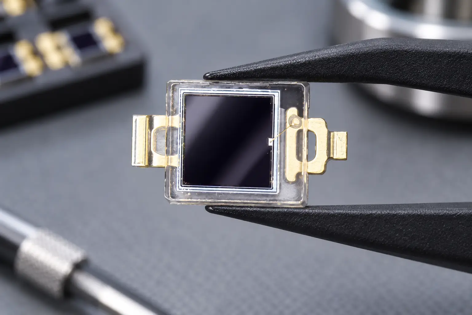
Si PIN photodiode PDCP08 Series PDCP08-511
The PDCP08-511 is a high-performance Black Epoxy PIN Photodiode designed for precision infrared applications. Encased in a special black epoxy resin, this sensor effectively acts as a daylight filter, blocking visible light interference while maximizing sensitivity at 940nm. With a large 2.9×2.9mm active area and low dark current, it ensures reliable signal detection for optical switches and remote control systems, even in noisy ambient light environments.
3. Spectral Alignment: 850nm vs. 940nm Optical Transmission Links
Selecting the wrong wavelength is an easy mistake when building an IR photodiode emitter pair. While standard silicon responds across the 400nm to 1100nm band, standardizing on either 850nm or 940nm involves specific design trade-offs.
Spectral Wavelength Trade-Offs:
- 850nm Optical Link: Delivers higher silicon responsivity (~0.55 to 0.62 A/W) and higher optical signal strength, but produces a faint visible red glow in darkness.
- 940nm Optical Link: Fully invisible to the human eye, matches the atmospheric moisture absorption dip for lower solar interference outdoors, but yields moderate silicon responsivity (~0.40 to 0.50 A/W).
Silicon PIN Photodiode Responsivity Differences
Silicon detectors hit peak responsivity between 850nm and 900nm.
- At 850nm, a typical photodiode delivers a responsivity around R = 0.58 A/W.
- At 940nm, that same silicon chip drops to around R = 0.42 A/W.
Operating an IR photodiode emitter pair at 850nm nets roughly 30% to 40% more raw photocurrent for the same received optical power. If your product stays indoors and operates on a tight battery power budget, an 850nm link gives you better energy efficiency.
Ambient Sunlight and Outdoor Interference
If your product operates outdoors or near direct sunlight, the 850nm responsivity advantage disappears. Solar radiation reaches sea level with deep spectral absorption notches caused by atmospheric water vapor and gases.
One of these natural water vapor absorption dips centers at 940nm. Solar background irradiance drops sharply right at this wavelength.
Even though a 940nm IR photodiode emitter pair generates lower raw photocurrent, ambient optical solar noise drops even faster. As a result, your overall signal-to-noise ratio (SNR) outdoors is substantially higher at 940nm than at 850nm.
Eliminating Ambient Visible Light Interference
Ambient room lighting, fluorescent tubes, and direct sunbeams will drive an unfiltered photodiode into early saturation. If the DC photocurrent pushes the amplifier output to the supply rail, your sensor stops reading real signal transitions.
Daylight Blocking Mechanism:
Visible Spectrum (400nm – 700nm) ➔ Blocked completely by dark resin
Infrared Band (850nm – 940nm) ➔ Passes freely with over 85% transmission efficiency
The simplest defense is integrating an optical high-pass or bandpass daylight-blocking filter into the receiver packaging. The black epoxy PIN photodiode PDCP08-511 uses a cast black epoxy resin that absorbs visible wavelengths below 750nm while transmitting infrared photons above 820nm with minimal insertion loss. This lets your IR photodiode emitter pair operate reliably under heavy ambient lighting without requiring expensive external optical filters.
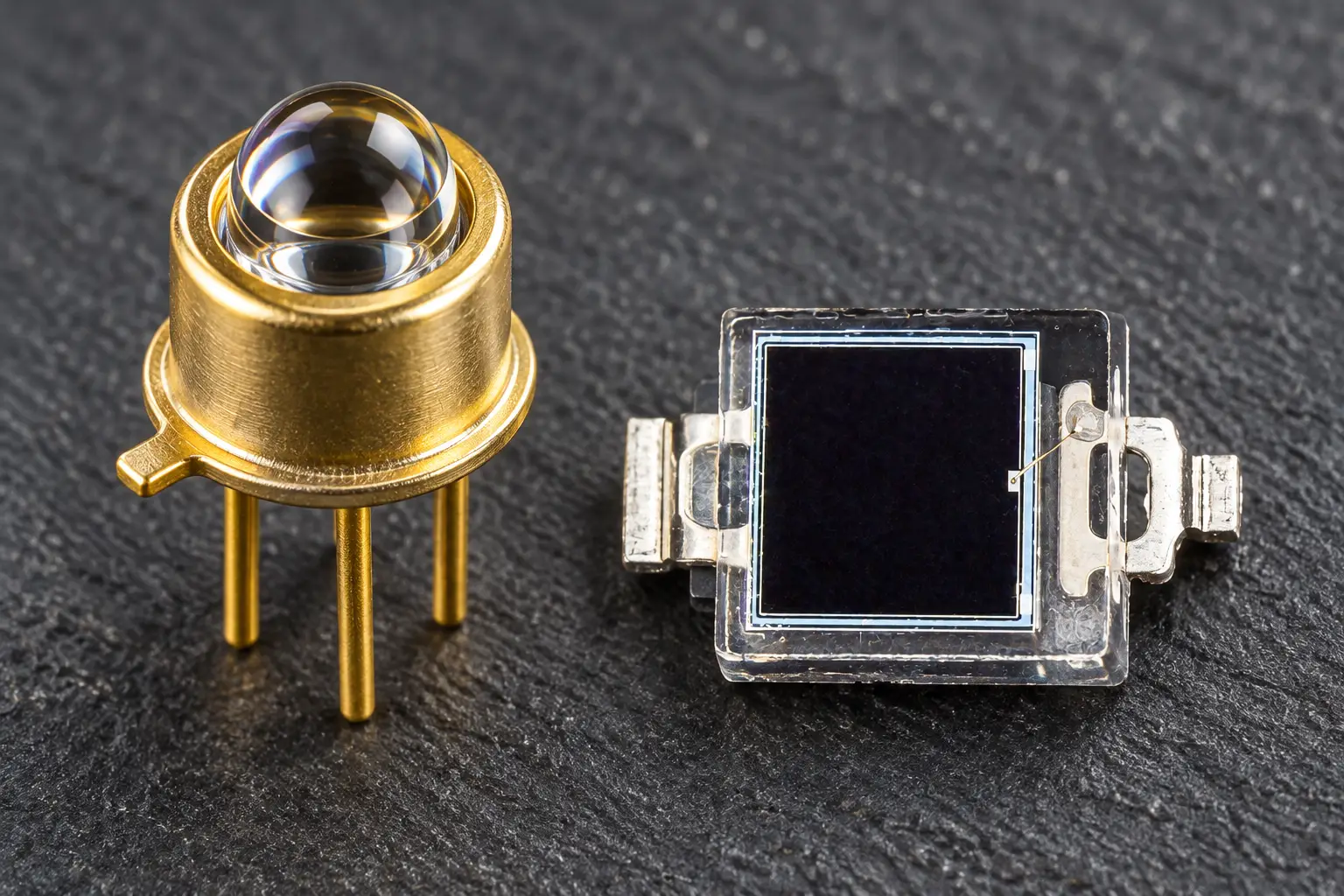
4. Packaging Selection: TO-Can vs. Surface Mount Devices (SMD)
Choosing between hermetic metal cans and plastic surface-mount packages affects thermal balance, mechanical life, and manufacturing costs.
| Engineering Parameter | TO-Can Package (TO-18, TO-46, TO-39) | SMD Package (1206, Side-looker, Molded Leadframe) |
|---|---|---|
| Thermal Dissipation | Superior thermal conduction (R_th < 80 °C/W) | Moderate heat dissipation, heavily dependent on PCB copper |
| Hermetic Protection | True glass-to-metal seal (Mil-STD compliant) | Non-hermetic, vulnerable to humidity and resin yellowing |
| Optical Window | Precision spherical ball lens or flat optical glass | Cast clear/black epoxy dome or flat transfer-molded lens |
| Assembly Method | Through-hole wave soldering or manual insertion | High-speed automated surface-mount pick-and-place |
| Unit Cost Profile | Higher bill-of-materials unit cost | Highly competitive cost structure for volume consumer builds |
| Operating Temperature | -40°C to +125°C continuous rating | -40°C to +85°C (specialized models rated to +105°C) |
When to Select TO-Cans
For harsh industrial instrumentation, agricultural sensors, oil and gas detection, or high-reliability outdoor perimeters, TO-can packaging remains the gold standard.
A metal-can IR photodiode emitter pair isolates delicate semiconductor dies from moisture ingress, airborne chemicals, and thermal shock. The rigid kovar header provides stable grounding against electromagnetic interference (EMI). If you need to drive the infrared LED at high forward currents, a TO-can dissipates heat far better than standard PCB plastic footprints.
When to Select SMD
When size, weight, and automated manufacturing dictate design choices, SMD packages win out. Modern SMD side-view and top-view designs provide consistent optical beam accuracy that rivals standard through-hole LEDs.
When laying out an SMD IR photodiode emitter pair, pay close attention to thermal relief. As an infrared LED die warms up during operation, its optical output power drops by roughly -0.3% to -0.5% per degree Celsius. Meanwhile, the photodiode reverse dark current roughly doubles for every 8°C to 10°C rise in junction temperature.
Isolate the emitter thermally from the photodiode on your circuit board using thermal breaks, ground relief cutouts, or isolated copper pours to keep thermal crosstalk under control.
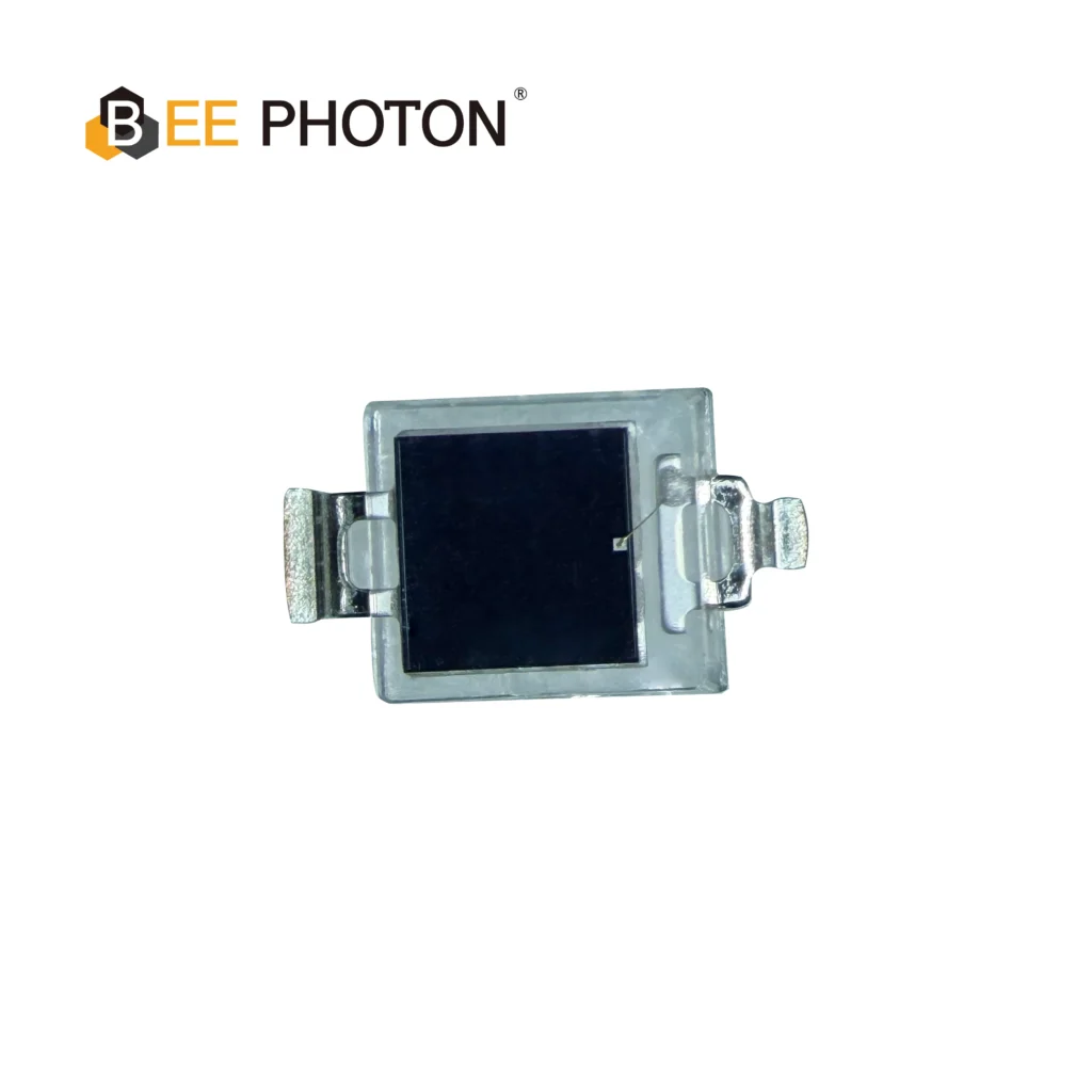
Si PIN photodiode PDCP08 Series PDCP08-501
High-Performance Detection: The PDCP08-501 is a high-speed Silicon PIN Photodiode with a transparent window.
Key Specs: Featuring a 2.9×2.9mm active area, this PIN photodiode offers low dark current and high responsivity, making it an ideal sensor for general optical switches and light detection systems.
5. Receiver Conditioning: Transimpedance Amplifier (TIA) Circuit Matching
Selecting a matched IR photodiode emitter pair is only half the battle. If your analog front-end (AFE) circuit is unstable, you will spend weeks hunting phantom oscillations or sluggish signal fall times.
Operational Biasing Modes:
- Photovoltaic Mode (Zero Bias, V_bias = 0V): Yields virtually zero dark current and minimal Johnson noise. Best for precision DC measurement and low-drift sensing, though junction capacitance remains high.
- Photoconductive Mode (Reverse Bias, V_bias = -3V to -15V): Drops photodiode junction capacitance by 60% to 80%, expanding frequency response into the megahertz band. Ideal for high-speed pulse detection at the cost of elevated reverse dark current.
Transimpedance Amplifier Topology Summary:
Inverting Node: Photodiode cathode enters the inverting input of the operational amplifier.
Feedback Loop: Resistor R_f in parallel with stabilization capacitor C_f connects the amplifier output back to the inverting input.
Non-Inverting Node: Connected directly to analog ground (photovoltaic mode) or a stable reference voltage.
As detailed in analog design references like the Analog Devices TIA Design Guide, stabilizing an operational amplifier against photodiode junction capacitance requires balanced feedback compensation.
Designing the Transimpedance Gain and Feedback Loop
Your amplifier converts incoming photocurrent into an output voltage using a transimpedance feedback resistor:
V_out = I_ph * R_f
To prevent the amplifier from oscillating due to the phase lag introduced by detector junction capacitance, add a tiny feedback capacitor C_f in parallel with R_f.
Calculate the feedback capacitor value using the geometric mean approach:
C_f = sqrt( C_in / ( 2 * pi * R_f * GBW ) )
Where:
- C_in is the total input capacitance at the inverting terminal: C_in = C_j + C_amp_differential + C_amp_common_mode + C_trace.
- C_j is the internal junction capacitance of the photodiode die (found on the component datasheet).
- R_f is the transimpedance feedback resistor in ohms.
- GBW is the gain-bandwidth product of the selected operational amplifier in hertz.
The resulting signal bandwidth of the transimpedance amplifier stage is:
f_cutoff = 1 / ( 2 * pi * R_f * C_f )
If you choose a photodiode with an unnecessarily large active area to catch a wide beam, C_j climbs from 4pF up to 100pF or more. That capacitance spike forces you to increase C_f to prevent phase ringing, which can severely choke your usable system bandwidth.
A well-matched IR photodiode emitter pair pairs a tighter emitter beam with a smaller receiver active area, keeping C_j minimal and allowing your receiver circuit to achieve clean megahertz-range pulse response.
6. Field Case Studies: Solving Real-World Optical Link Failures
Case 1: Resolving False Triggers in a High-Speed Industrial Sorting Gate
A package logistics company ran into an issue where an automated conveyor sorter dropped detection pulses on light-colored poly mailers, but registered false positives on dark parcels.
- The Original Architecture: A wide-angle (120°) surface-mount 850nm LED paired with a broad-spectrum clear-molded photodiode.
- The Root Cause: The wide emitter beam scattered off dusty conveyor side-rails, bouncing stray infrared light directly back into the unshielded clear detector. This background reflection elevated the baseline DC voltage near the transimpedance amplifier’s clipping rail. When a light parcel passed through, the extra reflection threw the amplifier into full saturation.
- The Engineering Fix: We replaced the wide configuration with a focused IR photodiode emitter pair. The emitter was narrowed to a 20° beam, and the receiver was upgraded to a black epoxy PIN photodiode PDCP08-511. The black epoxy eliminated background factory lighting, while the tighter 20° optical beam kept stray reflections off the conveyor rails. The design gave the system a 14dB boost in signal-to-noise ratio, completely clearing up false triggers on the sorting line.
Case 2: Eliminating Outdoor Glare Failure in Automated Access Gates
A gate barrier system performed reliably indoors on the test bench, but failed continuously once installed on an outdoor test track in sunny Arizona. At midday, the barrier gate refused to close, interpreting normal sunlight as an unbroken vehicle obstruction beam.
- The Original Architecture: A high-power 850nm emitter paired with a clear-molded planar photodiode operating in simple continuous-wave (CW) DC mode across a 3-meter driveway.
- The Root Cause: Ambient sunlight swamped the clear silicon photodiode. Sunlight at 850nm generated roughly 1.8mA of baseline DC photocurrent, driving the receiver circuit to ground rail lockup regardless of whether an obstacle broke the beam.
- The Engineering Fix: The engineering team rebuilt the link around an outdoor-optimized IR photodiode emitter pair. They switched wavelengths from 850nm to 940nm, shifting the operating point directly into the solar atmospheric moisture absorption notch.
On the driver side, the continuous DC beam was changed to a 10kHz pulsed LED drive at a 5% duty cycle. The receiver was updated with an active AC-coupled bandpass filter tuned to 10kHz. This allowed the circuit to reject the heavy steady-state solar DC photocurrent while passing the modulated infrared signal cleanly through to the gate controller logic.
7. Why Sourcing Matched Pairs Beats Fragmented Purchasing
Procuring emitters from one semiconductor vendor and hunting down photodiodes from another frequently leads to silent batch-to-batch failures on your production line.
Common Supply Chain Risks in Fragmented Sourcing:
- Uncoordinated forward voltage (Vf) variations across different LED foundry lots.
- Uncontrolled spectral center drift shifting the emitter peak out of the photodiode peak band.
- Mechanical lens mold variations altering optical centerlines relative to PCB mounting pads.
- Disjointed minimum order quantities (MOQs) leaving assembly lines short on critical matching parts.
When you work with a vertically integrated optoelectronic design and manufacturing partner like BeePhoton, you eliminate the headache of cross-vendor part matching.
We align the radiometric performance, angular emission tolerances, and optical acceptance profiles of every IR photodiode emitter pair before components reach your assembly floor. Instead of spending your design cycles debugging beam alignment margins and ambient light clipping on the test bench, you receive paired emitter and photodiode sets built to drop straight into your production line.

Si PIN photodiode PDCP08 Series PDCP08-502
The PDCP08-502 is a high-response 2.9×2.8mm Silicon PIN Photodiode designed for precision photoelectric applications. Featuring low junction capacitance, low dark current, and a wide spectral range (340-1100nm), it is the ideal component for optical switches and compact sensing modules requiring stable and fast signal output.
Frequently Asked Questions (FAQ)
What is the most reliable way to prevent ambient sunlight from saturating an IR photodiode emitter pair?
The best defense combines optical and electronic filtering:
1.Optical Filtering: Use an infrared detector encapsulated in visible-light-blocking black epoxy, such as the PDCP08-511, to strip out ambient wavelengths below 750nm.
2.AC Modulation: Modulate your emitter LED with a carrier frequency (typically between 10kHz and 40kHz) instead of driving it with a flat DC current.
3.Electronic Filtering: Place a high-pass or active bandpass filter right after the transimpedance amplifier to strip out remaining 50Hz/60Hz mains hum and steady-state solar DC drift, amplifying only your modulated carrier pulses.
How does changing from an 850nm to a 940nm IR photodiode emitter pair affect circuit gain?
Silicon PIN photodiodes have lower spectral responsivity at 940nm (roughly 0.42 A/W) than at 850nm (roughly 0.58 A/W), meaning your receiver will generate about 25% to 35% less photocurrent for an identical incoming radiant power level. To restore your target output voltage swings without overdriving the 940nm LED, increase your transimpedance feedback resistor R_f by roughly 30% to 40%, and recalculate your feedback capacitor C_f to preserve overall loop stability.
Why does my IR photodiode emitter pair lose signal strength when the ambient operating temperature rises?
This drop-off comes from temperature effects at both ends of the optical link:
1.The Infrared LED: Standard GaAs and AlGaAs infrared emitters exhibit a negative thermal coefficient. Radiant output power typically drops between -0.3% and -0.5% for every degree Celsius rise in junction temperature.
2.The Silicon Photodiode: While photodiode responsivity at 850–940nm actually climbs slightly with temperature, dark leakage current doubles roughly every 8°C to 10°C.
Without thermal isolation, the combination of declining emitter power and rising detector leakage noise degrades your system’s dynamic range and signal-to-noise ratio over wide temperature swings.
Partner with BeePhoton for Matched Optoelectronic Solutions
Getting consistent performance from an IR photodiode emitter pair requires a solid grasp of optical beam geometry, silicon physics, and analog front-end design. Whether you are balancing narrow 4° light curtains, selecting diffuse wide-angle sensors, or working around harsh solar glare, component matching makes all the difference.
Stop wasting engineering hours guessing whether catalog emitters and detectors will work together on your production line.
- Explore our complete catalog of bare-die and custom-packaged silicon PIN photodiodes.
- Request matched component samples for your initial engineering prototype validation.
- Contact our engineering team directly at info@photo-detector.com or through our BeePhoton Contact Portal to discuss custom radiant matching, custom lens assemblies, and one-stop sourcing tailored to your optical sensing setup.