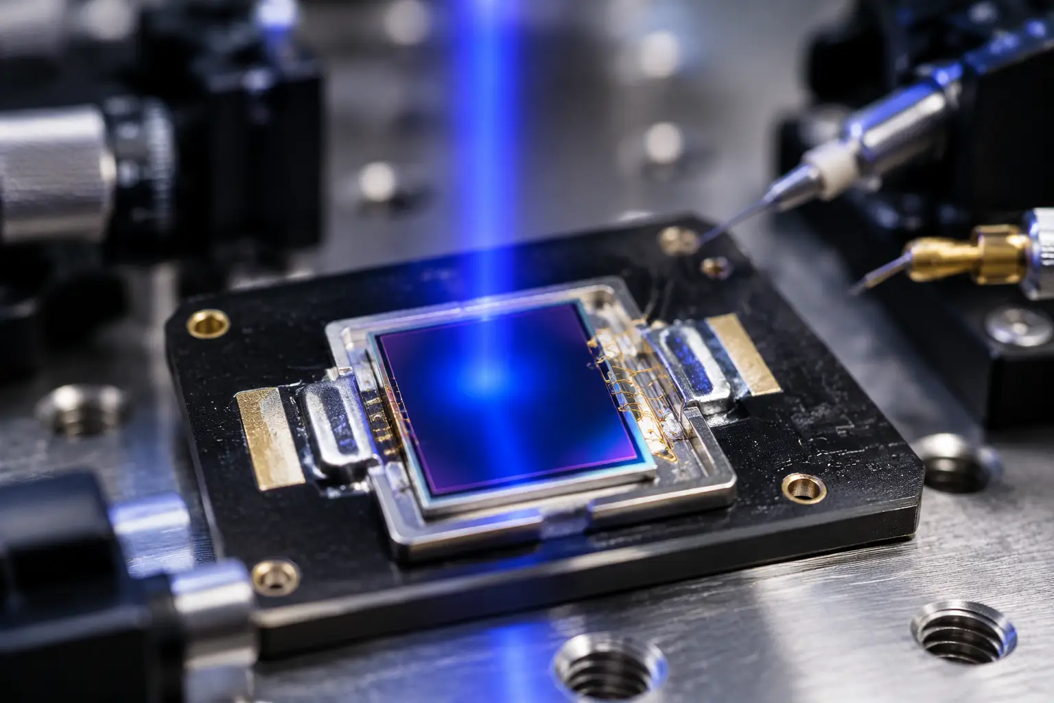
If you have spent more than an hour at a hardware bench trying to coax clean 10 MHz or 50 MHz pulses out of an optical receiver, you know the drill. You calculate your feedback resistor, pick what looks like a screamer of an op-amp with hundreds of megahertz of gain-bandwidth product, power up the rail, hook up your light source, and hit auto-scale on the scope.
Instead of a clean, sharp pulse response, you get a 65 MHz sine wave humming away at rail-to-rail levels. Or worse: a mushy, slow step response that looks like someone dragged your signal through cold molasses, followed by three cycles of violent ringing.
You check your power supply rails. Clean. You inspect your bypass caps. Solder joints look solid. So why is the transimpedance amplifier (TIA) acting like a Colpitts oscillator?
Nine times out of ten, the culprit sitting silently on your copper is the photodiode junction capacitance Cj.
When engineers design analog front ends (AFE) for optical sensing, pulse oximetry, LIDAR, or industrial flame detection, they usually obsess over the photodiode’s responsivity and dark current. Those matter, sure. But if you ignore your photodiode junction capacitance Cj, the parasitic physics of your silicon detector will wreck your loop phase margin before the signal ever makes it past your first amplification stage.
Let’s walk through how photodiode junction capacitance Cj actually interacts with your amplifier loop, how dropping your capacitance from 70pF down to 15pF (or lower) rescues circuit cutoff bandwidth, and what you can do on your PCB right now to keep your optical front-ends quiet, fast, and rock-solid stable.
The Root Problem: Why Your TIA Loop Hates Input Capacitance
A transimpedance amplifier converts an input current from a photodiode into an output voltage. In textbook schematics, it looks deceptively simple: one operational amplifier, one feedback resistor Rf, and a photodetector diode pointing toward the inverting terminal.
Reality check from the lab bench: ideal op-amps do not exist, and zero-capacitance diodes are a fantasy. The photodiode junction capacitance Cj forms a low-pass filter with your feedback resistor in the feedback path, which turns into a zero in your noise-gain transfer function. That zero eats your phase margin alive.
To see what is happening under the hood, look at the total input capacitance Cin hanging off the inverting node:
Cin = photodiode junction capacitance Cj + Ccm + Cdiff + Ctrace
Where:
- photodiode junction capacitance Cj is the depletion layer capacitance of the reverse-biased or zero-biased diode.
- Ccm is the common-mode input capacitance of the op-amp.
- Cdiff is the differential input capacitance of the op-amp.
- Ctrace is your stray PCB layout parasitic capacitance (usually 1 pF to 3 pF if you know what you are doing, 8 pF if you poured copper ground planes directly under the inverting pin).
In almost every photodetector circuit using standard optical detectors, photodiode junction capacitance Cj is the monster in the room. While your op-amp might contribute 1.5 pF of input capacitance, a large-area photodiode running at zero bias can easily inject a photodiode junction capacitance Cj of 70pF, 120pF, or even 300pF directly onto the sensitive summing node.
According to classical loop stability theory detailed in Texas Instruments’ TIA stability application notes, this total input capacitance introduces a zero in the noise gain (1/beta) curve at a specific frequency:
fz = 1 / (2 * pi * Rf * Cin)
Because photodiode junction capacitance Cj dominates Cin, a high photodiode junction capacitance Cj pushes fz down into lower frequencies. As the noise gain rises at +20 dB/decade, it slams directly into the amplifier’s open-loop gain (Aol) curve at a closing rate of 40 dB/decade.
When your rate-of-closure hits 40 dB per decade, your phase margin drops close to zero. The result? Your amplifier rings like a church bell, exhibits extreme gain peaking, or turns into an outright autonomous RF oscillator.
The Math You Actually Need on the Bench: Bandwidth vs. Capacitance
Most application notes hand you idealized equations that fall apart when your component tolerances drift. But you still need a baseline analytical target when sizing your photodiode and feedback compensation capacitor Cf.
The closed-loop -3dB bandwidth of a properly compensated transimpedance amplifier does not scale linearly with op-amp gain bandwidth product (GBW). It is throttled by your feedback resistor and your total input capacitance, which is primarily dictated by your photodiode junction capacitance Cj.
The Achievable -3dB Bandwidth Formula
Assuming you tune your feedback capacitor Cf to yield a classic 45-degree or 65-degree Butterworth or Bessel phase response, the maximum achievable -3dB transimpedance bandwidth is defined by:
f(-3dB) = sqrt( GBW / (2 * pi * Rf * Cin) )
Notice that photodiode junction capacitance Cj sits inside Cin in the denominator underneath a square root.
If you have a photodiode junction capacitance Cj of 70pF, your denominator is massive. If you find a way to drop that photodiode junction capacitance Cj down to 15pF, look at what happens to your bandwidth: you get more than double the usable cutoff frequency without burning a single extra milliamp of supply current on a faster, more expensive operational amplifier.
Calculating the Feedback Capacitor Cf
To prevent that rising noise-gain zero from destroying stability, you must drop a small feedback capacitor Cf in parallel with your feedback resistor Rf. This inserts a pole in the noise gain curve to level off the loop gain:
fp = 1 / (2 * pi * Rf * Cf)
For a maximally flat 45-degree phase margin Butterworth response, the standard design equation from Analog Devices’ MT-059 optical tutorial dictates:
Cf = sqrt( Cin / (2 * pi * Rf * GBW) )
Let’s plug in real hardware numbers to see why managing photodiode junction capacitance Cj is so critical.
- Scenario A (High Cj): Rf = 100 kOhm, GBW = 50 MHz, and photodiode junction capacitance Cj = 70pF (with 3pF parasitics, Cin = 73pF).
Cf = sqrt( 73e-12 / (2 * pi * 100e3 * 50e6) ) = sqrt( 73e-12 / 3.14159e13 ) = 1.52 pF.
Achievable Bandwidth f(-3dB) = sqrt( 50e6 / (2 * pi * 100e3 * 73e-12) ) = 1.04 MHz. - Scenario B (Low Cj): Rf = 100 kOhm, GBW = 50 MHz, and photodiode junction capacitance Cj = 15pF (with 3pF parasitics, Cin = 18pF).
Cf = sqrt( 18e-12 / (2 * pi * 100e3 * 50e6) ) = sqrt( 18e-12 / 3.14159e13 ) = 0.75 pF.
Achievable Bandwidth f(-3dB) = sqrt( 50e6 / (2 * pi * 100e3 * 18e-12) ) = 2.10 MHz.
By cutting photodiode junction capacitance Cj from 70pF to 15pF, you literally double your signal bandwidth. At the same time, because your required feedback capacitor Cf drops, you reduce your high-frequency noise gain peaking, delivering a much cleaner signal-to-noise ratio (SNR) at your digitizer or ADC.

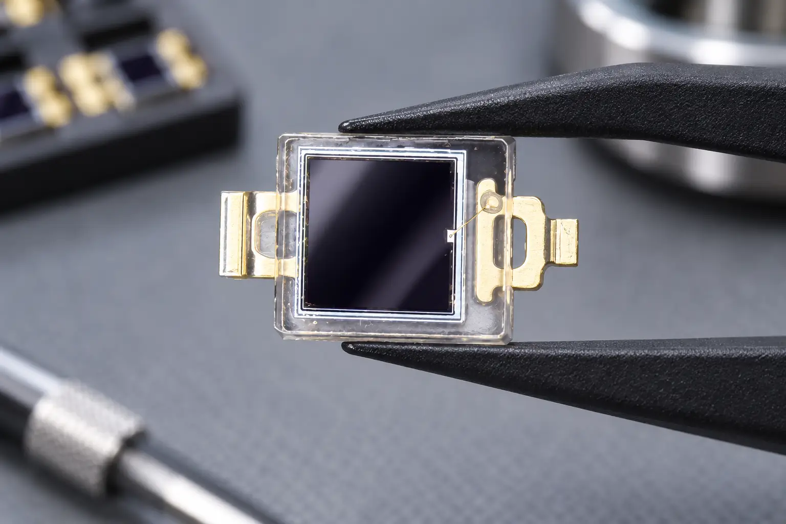
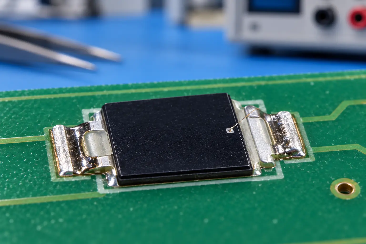
Si PIN photodiode PDCP08 Series PDCP08-511
The PDCP08-511 is a high-performance Black Epoxy PIN Photodiode designed for precision infrared applications. Encased in a special black epoxy resin, this sensor effectively acts as a daylight filter, blocking visible light interference while maximizing sensitivity at 940nm. With a large 2.9×2.9mm active area and low dark current, it ensures reliable signal detection for optical switches and remote control systems, even in noisy ambient light environments.
Where Does Photodiode Junction Capacitance Cj Come From?
To control photodiode junction capacitance Cj, you have to understand the physical semiconductor structure generating it.
A silicon photodiode is essentially a PN or PIN junction. The depletion region between the P-doped and N-doped silicon behaves as an insulating dielectric sandwiched between two conductive plates. The basic parallel-plate capacitance equation explains everything:
Cj = (epsilon_0 * epsilon_r * A) / W
Where:
- epsilon_0 is the permittivity of free space.
- epsilon_r is the relative permittivity of silicon (around 11.7 to 11.9).
- A is the active photosensitive area of the detector die.
- W is the width of the depletion layer.
Silicon PIN Junction Cross-Section Layering:
- Incident Light (hv): Enters through the anti-reflective window coating on the front surface.
- Anode Contact (P+ Layer): Heavily doped top conductive silicon layer.
- Depletion Region (Intrinsic Layer, Width = W): Acts as the dielectric spacer. Expanding W directly drops photodiode junction capacitance Cj.
- Cathode Contact (N+ Substrate): Heavily doped bottom substrate contact leading to the external cathode pin.
From this basic physics relationship, you have two physical knobs you can turn to minimize photodiode junction capacitance Cj:
- Shrink the active area (A): If your optical beam spot is only 0.8 mm in diameter, using a 5 mm x 5 mm detector die is bad engineering. You are buying yourself massive photodiode junction capacitance Cj with zero added responsivity, since the extra silicon area only collects ambient stray light and generates dark current noise.
- Widen the depletion layer (W): You widen the depletion layer either by manufacturing a PIN diode with an intrinsic (I) layer or by applying an external reverse bias voltage (Vbias) across the junction.
Junction Capacitance vs. Reverse Bias Voltage
The following breakdown illustrates how depletion width and capacitance behave under progressive reverse voltage levels for a typical medium-area silicon PIN detector:
| Applied Reverse Bias (Vbias) | Depletion Zone State | Depletion Layer Width (W) | Typical Photodiode Junction Capacitance Cj |
|---|---|---|---|
| 0 V (Photovoltaic Mode) | Built-in potential only | Minimum thickness | ~75 pF to 90 pF |
| -2 V Reverse Bias | Partial depletion growth | 2.5x expansion | ~35 pF |
| -5 V Reverse Bias | Substantial depletion extension | 4.5x expansion | ~18 pF |
| -10 V Reverse Bias | Near-full depletion of I-layer | 6.0x expansion | ~14 pF |
| -20 V Reverse Bias | Saturated full depletion region | Maximum limit reached | ~12 pF (Asymptotic floor) |
As shown above, your photodiode junction capacitance Cj drops dramatically over the first few volts of reverse bias before leveling out once the intrinsic region is fully depleted.
Tactical Levers to Slash Photodiode Junction Capacitance Cj
When an AFE engineer tells me their transimpedance stage is oscillating at 40 MHz or cutting off their pulses, we go through a checklist of practical silicon and circuit adjustments to bring down photodiode junction capacitance Cj.
1. Photovoltaic vs. Photoconductive Mode: Applying Reverse Bias
Operating a photodetector in photovoltaic mode (zero bias, Vbias = 0V) gives you the lowest possible dark current and zero DC offset from leakage. It is great for low-speed DC precision light meters. But for high-speed circuits, zero-bias is your worst enemy because your photodiode junction capacitance Cj is at its absolute maximum.
When you switch to photoconductive mode by applying a reverse bias voltage to the photodiode cathode (for standard N-on-P silicon), you physically sweep mobile carriers out of the junction, expanding the depletion layer thickness W.
As documented in standard PIN diode literature, reverse-biasing a silicon PIN diode can easily slash your photodiode junction capacitance Cj by a factor of 4x to 8x.
Engineering warning: Reverse bias is not a free lunch. As you increase reverse bias voltage, your reverse leakage current (dark current, Id) climbs exponentially. That dark current introduces shot noise (In_shot = sqrt(2 * q * Id * B)) and creates a DC offset voltage across your feedback resistor (Vout_offset = Id * Rf). You must balance your phase margin gains against your DC error budget.
2. Selecting the Right Silicon Geometry and Packaging
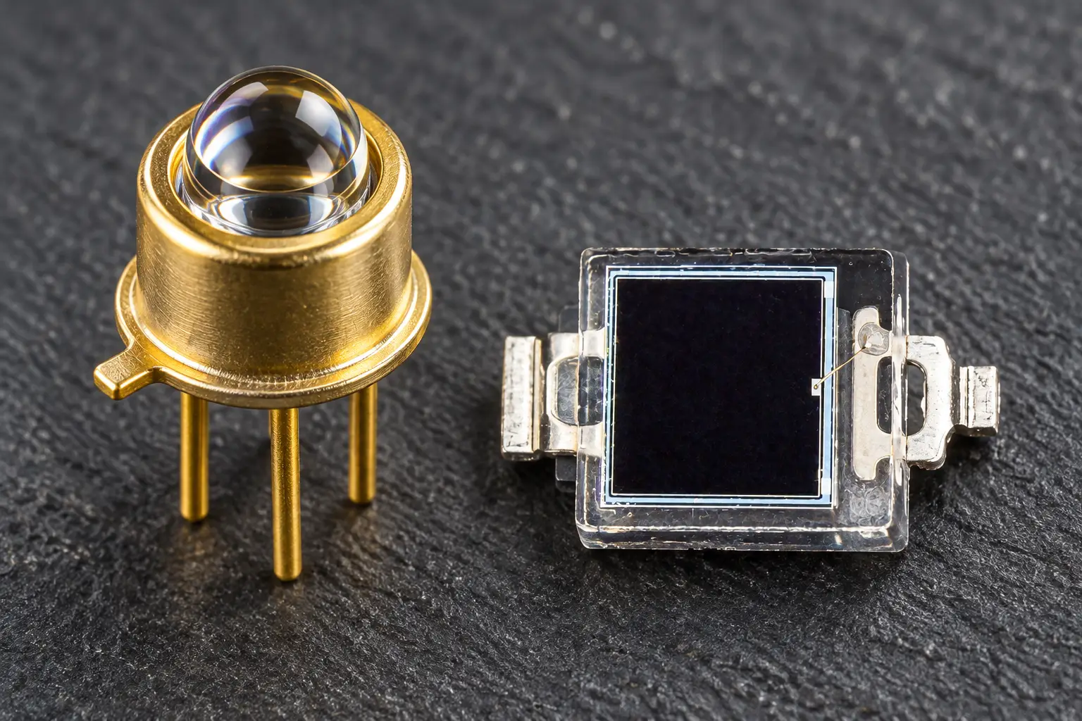
Don’t use a massive general-purpose diode when a high-speed detector exists for your spectral band. Packaging also contributes package parasitic capacitance parallel to photodiode junction capacitance Cj.
At BeePhoton, photodetector architectures are optimized to minimize intrinsic junction capacitance while maintaining wide responsivity windows across visible and near-infrared (NIR) spectra.
Here is how three standard photodiode configurations stack up when evaluating photodiode junction capacitance Cj for high-speed transimpedance stages:
| Photodiode Model | Active Area Size | Typical Peak Responsivity | Photodiode Junction Capacitance Cj (0V Bias) | Photodiode Junction Capacitance Cj (Reverse Biased) | Best AFE Application Match |
|---|---|---|---|---|---|
| PDCP08-511 | Daylight filter epoxy package | 940 nm (NIR optimized) | ~72 pF | ~16 pF (@ -5V) | Ambient light rejection, high-speed optical switches, IR telemetry |
| PDCP08-502 | 2.9 mm x 2.8 mm footprint | 850 nm – 940 nm | ~68 pF | ~14 pF (@ -10V) | Pulse oximetry AFE, medical sensors, precision pulse timing |
| PDCP08-501 | Compact surface-mount die | 400 nm – 1100 nm broadband | ~28 pF | ~5 pF (@ -15V) | High-speed optical transceivers, laser pickup, transient analyzers |
When you review this comparison, notice how moving from zero-bias to a modest 5V or 10V reverse bias drops your photodiode junction capacitance Cj down from 70pF levels to the sub-15pF sweet spot.
If you are dealing with tight power rails and cannot provide a -10V bias supply, choosing a diode with a smaller native die area like the PDCP08-501 Silicon PIN gives you low baseline photodiode junction capacitance Cj even under low-bias operation.
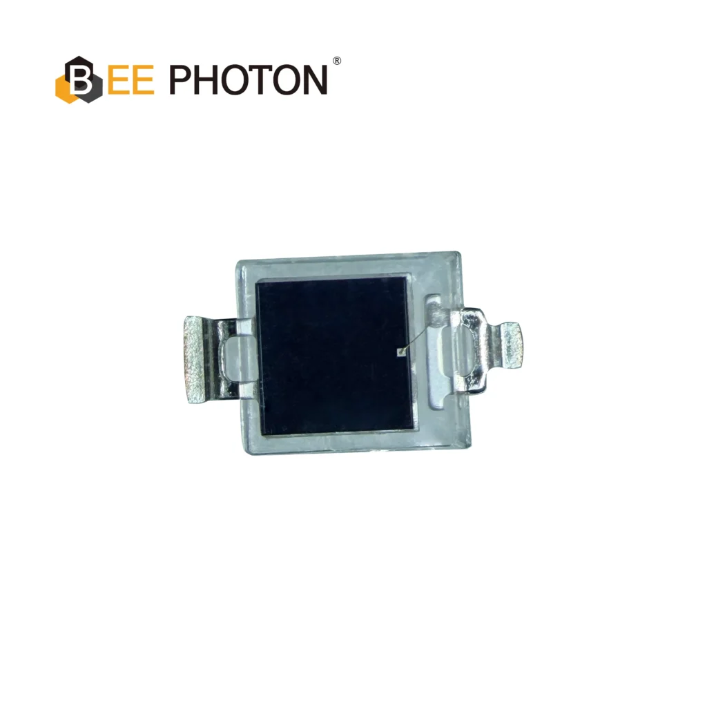
Si PIN photodiode PDCP08 Series PDCP08-501
High-Performance Detection: The PDCP08-501 is a high-speed Silicon PIN Photodiode with a transparent window.
Key Specs: Featuring a 2.9×2.9mm active area, this PIN photodiode offers low dark current and high responsivity, making it an ideal sensor for general optical switches and light detection systems.
PCB Layout Traps That Ruin Your Capacitance Optimization
You can spend days sourcing a premium PIN photodiode with an ultra-low photodiode junction capacitance Cj, only to completely ruin your circuit bandwidth because your PCB layout engineer treated the photodiode trace like a standard digital signal net.
Every picofarad you add on the PCB summing trace adds directly to your photodiode junction capacitance Cj. Here are the cardinal rules for routing high-speed photodiode front ends:
1. Strip the Ground and Power Planes Under the Summing Node
Copper pours on internal layers under your inverting input trace create parasitic parallel-plate capacitance to ground. A standard 0.062-inch (1.6mm) 4-layer FR4 board with ground on Layer 2 produces roughly 1 pF of parasitic capacitance for every 0.1 inch of standard trace length.
If you leave copper poured directly beneath the summing pin of your op-amp and your photodiode anode pad, you can accidentally add 5pF to 10pF of parasitic capacitance right alongside your photodiode junction capacitance Cj.
To maintain low parasitic summing node capacitance, follow this PCB layer stackup strategy:
- Layer 1 (Top Signal): Mount photodiode pad directly adjacent to the op-amp inverting pin with feedback resistor Rf and feedback capacitor Cf spanning across them.
- Layer 2 (Internal Ground Plane): Cut a copper void window directly beneath the photodiode pads, inverting pin, and Rf/Cf pads.
- Layer 3 (Internal Power Plane): Extend the same copper void window across Layer 3 to prevent inter-plane capacitive coupling.
- Layer 4 (Bottom Signal/Ground): Keep the voided area clear of any high-speed digital lines or noisy switching power nets.
2. Minimize Trace Length Between Cathode/Anode and the Op-Amp
Keep the photodiode within a couple of millimeters of the op-amp inverting pin. Long traces do not just add capacitive parasitics parallel to photodiode junction capacitance Cj; they also act as antennas picking up 2.4 GHz Wi-Fi, switch-mode power supply ripple, and digital clock spikes.
3. Route Guard Rings Around the High-Impedance Node
If you are operating your photodiode in photoconductive mode with a reverse bias voltage, surface leakage currents across dirty flux residue on your board will leak into your inverting node.
Surround the trace connecting your photodiode to the op-amp input with a guard trace driven at the same electrical potential (for an inverting TIA with the non-inverting pin grounded, the guard ring must be tied to a quiet analog ground).
A Bench War Story: Calming a 55 MHz Ringing Optical AFE
A few years ago, I had a client building a custom multi-wavelength optical spectrometer for sorting recycled plastics. Their optical receiver chain was designed around an ultra-low-noise FET-input op-amp with a 120 MHz GBW, driving an Rf of 250 kOhm.
When they illuminated their photodetector with pulsed laser diodes, their scope showed massive ringing at 55 MHz, riding right on the leading edge of their measurement pulse. The settling time was over 180 nanoseconds—completely blowing past their 40 ns measurement window.
The team assumed their operational amplifier had bad decoupling. They threw ferrite beads, multi-layer ceramic capacitors, and ground-strap modifications at the board. Nothing worked.
We hooked the board up to a network analyzer and measured the actual capacitance hanging off the inverting terminal.
The engineer had selected a budget, large-area silicon photodiode running at zero-bias. The datasheet stated a “typical” photodiode junction capacitance Cj of 75pF. On the actual manufactured batch, the zero-bias photodiode junction capacitance Cj was closer to 88pF.
Combine that with 4pF of sloppy trace layout and 2pF of op-amp input capacitance, and their total Cin was 94pF.
Their noise-gain zero fz sat way down at:
fz = 1 / (2 * pi * 250e3 * 94e-12) = 6.77 kHz
Because fz was positioned so low in frequency, their noise gain slammed into the open-loop gain curve at a severe closing angle. Their phase margin was down around 12 degrees.
The Simple Fix
Instead of redesigning the whole board around a different op-amp architecture, we executed two targeted changes:
- Swapped the Photodiode: We replaced their generic detector with a PDCP08-502 Silicon PIN. We routed an isolated -5V clean linear bias supply to reverse-bias the photodiode cathode. Under -5V bias, its photodiode junction capacitance Cj dropped down to approximately 14pF.
- Re-Tuned Feedback Compensation: With the total input capacitance Cin lowered from 94pF to roughly 18pF (14pF photodiode junction capacitance Cj + 4pF parasitics), we recomputed our feedback compensation capacitor Cf:
Cf = sqrt( 18e-12 / (2 * pi * 250e3 * 120e6) ) = sqrt( 18e-12 / 1.88495e14 ) = 0.31 pF
We dropped a high-precision 0.3 pF RF-grade porcelain capacitor across the feedback resistor.
The result? The 55 MHz ringing completely disappeared on the next power-up. The pulse step response exhibited a clean 3% overshoot with a 45-degree Bessel-like settling behavior. The -3dB circuit bandwidth surged past 3.2 MHz, and their settling time collapsed from 180 ns down to under 28 ns.
The client did not need to buy an exotic 1 GHz RF op-amp. Controlling photodiode junction capacitance Cj solved the instability at the physical root.
Detailed Comparison: Circuit Behavior vs. Junction Capacitance
To show why optimizing photodiode junction capacitance Cj is your primary design lever, check how circuit parameters evolve as diode capacitance drops while keeping the feedback resistor Rf (100 kOhm) and op-amp (GBW = 50 MHz) identical:
| Photodiode Junction Capacitance Cj | Total Cin (Cj + 3pF parasitics) | Required Feedback Cap (Cf) | Resulting -3dB Bandwidth | Loop Phase Margin | Step Response Behavior |
|---|---|---|---|---|---|
| 120 pF (Large area, 0V bias) | 123 pF | 1.98 pF | 804 kHz | ~35 deg | Heavy ringing, slow settling time (>150 ns) |
| 70 pF (Medium area, 0V bias) | 73 pF | 1.52 pF | 1.04 MHz | ~45 deg | Moderate overshoot (~15%), usable but noisy |
| 25 pF (PIN diode, -3V bias) | 28 pF | 0.94 pF | 1.68 MHz | ~60 deg | Clean step, fast settling (<50 ns) |
| 15 pF (e.g. PDCP08-511 @ -5V) | 18 pF | 0.75 pF | 2.10 MHz | ~65 deg | Flat response, minimal peaking, high SNR |
| 5 pF (e.g. PDCP08-501 @ -15V) | 8 pF | 0.50 pF | 3.15 MHz | ~70 deg | Ultra-fast transient edge, zero visible oscillation |
If your hardware requirement calls for higher throughput, lower jitter, or faster edge detection, fighting photodiode junction capacitance Cj at the diode level gives you vastly superior power efficiency compared to brute-forcing the problem with power-hungry operational amplifiers.
SPICE Modeling: Don’t Trust Default Photodiode Models
Most engineers fire up LTspice or TINA-TI and pull a generic photodiode out of the library.
Default SPICE photodiode models almost always default to zero or an unrealistically low photodiode junction capacitance Cj like 2pF or 5pF unless you manually configure the model parameters (CJO, VJ, and M).
If you simulate your TIA circuit with an idealized 2pF photodiode model, your simulation will show a gorgeous 65-degree phase margin and a perfectly flat AC frequency curve. Then your bare PCBs arrive from the fab house, you solder on a physical detector with a 75pF photodiode junction capacitance Cj, and the board immediately starts humming at 50 MHz.
When building your simulation deck:
- Always manually place an explicit capacitor across your current source representing the actual photodiode junction capacitance Cj at your intended bias voltage.
- Include 1.5 pF of common-mode and differential op-amp input capacitance.
- Add 1.5 pF to 3 pF of stray board capacitance on the inverting node.
- Run an AC transfer function analysis and check the closed-loop noise gain curve. Look for any sharp peaking near your unity-gain crossover point. If you see a 6 dB to 12 dB peak in your AC amplitude, your circuit is on the verge of oscillation.
For detailed background on how to configure precise operational amplifier macromodels with realistic diode parasitics, check the engineering archives on IEEE Xplore or consult standard references on Transimpedance Amplifier stability criteria.

Si PIN photodiode PDCP08 Series PDCP08-502
The PDCP08-502 is a high-response 2.9×2.8mm Silicon PIN Photodiode designed for precision photoelectric applications. Featuring low junction capacitance, low dark current, and a wide spectral range (340-1100nm), it is the ideal component for optical switches and compact sensing modules requiring stable and fast signal output.
Practical Troubleshooting Guide: Spotting High Cj Issues on the Bench
When you are probing your prototype under a high-bandwidth digital storage oscilloscope, specific waveform signatures point directly to photodiode junction capacitance Cj problems rather than generic power supply noise or layout crosstalk:
Bench Signature 1: Damped High-Frequency Ringing on Pulse Edges
If an input optical pulse produces an initial edge followed by 3 to 6 ringing cycles at a single fixed frequency (typically between 20 MHz and 80 MHz), your feedback zero is undercompensated because your actual photodiode junction capacitance Cj is higher than the nominal value used to compute Cf.
Bench Signature 2: Peaking in the AC Frequency Response
Sweeping your optical source across frequency with a network analyzer will reveal a pronounced bump right before the -3dB roll-off. A gain peak of 3 dB or higher indicates less than 45 degrees of phase margin, which is a classic tell of excess photodiode junction capacitance Cj dragging down loop stability.
Bench Signature 3: Spurious Oscillations Disappearing Under Finger Touch
Touching the feedback network or the photodiode package with a plastic adjustment wand or a probe tip changes the stray capacitance. If the oscillation frequency shifts or disappears completely, the amplifier’s noise gain zero is unstable, and lowering photodiode junction capacitance Cj is your most reliable path to permanent stability.
Summary Checklist for Photodiode Junction Capacitance Optimization
Before you release your next photodetector front-end board to manufacturing, run through this bench-tested checklist:
- Have you checked the photodiode datasheet for the exact photodiode junction capacitance Cj at your operating reverse bias voltage, rather than relying on the zero-bias spec?
- Can your optical system tolerate a moderate reverse bias (such as -3.3V, -5V, or -12V) to slash photodiode junction capacitance Cj by 60% to 80%?
- Is your photodiode active area sized strictly to match your optical beam spot size to avoid collecting useless parasitic capacitance?
- Did you carve out internal power and ground copper planes directly underneath the op-amp inverting node and photodiode trace?
- Did you calculate your feedback capacitor Cf using real Cin values (including photodiode junction capacitance Cj + board parasitics) rather than guessing?
- Have you verified your phase margin with an AC sweep simulation including realistic photodiode junction capacitance Cj?
Frequently Asked Questions (FAQ)
What is the difference between photodiode junction capacitance Cj and shunt resistance Rsh?
Photodiode junction capacitance Cj is the reactive capacitance created across the depleted silicon PN junction, while shunt resistance (Rsh) represents the DC slope resistance of the un-illuminated diode around zero bias.
Rsh is typically very high (hundreds of megaohms to gigaohms for quality silicon). While shunt resistance dictates your baseline thermal Johnson noise at DC and low frequencies, photodiode junction capacitance Cj completely dominates the high-frequency stability, noise gain peaking, and -3dB bandwidth of your transimpedance amplifier.
Can I simply eliminate the feedback capacitor Cf if my photodiode junction capacitance Cj is very low?
Even if your photodiode junction capacitance Cj is tiny (say, 3pF to 5pF), completely omitting the feedback capacitor Cf is risky. Without any feedback capacitance, the stray parasitic capacitance across your feedback resistor (typically 0.1 pF to 0.3 pF for standard 0805 or 0603 surface mount chip resistors) will define your feedback pole.
If that parasitic capacitance is insufficient to compensate for your remaining photodiode junction capacitance Cj and op-amp input capacitance, you will still experience significant high-frequency gain peaking. It is always better practice to design with an intentional, temperature-stable C0G/NP0 capacitor for Cf.
Why does increasing reverse bias reduce photodiode junction capacitance Cj?
Applying an external reverse bias voltage pushes mobile majority carriers away from the PN junction: holes are pulled toward the negative bias terminal, and electrons are pulled toward the positive cathode contact.
This widens the depletion zone where no free carriers exist. Because junction capacitance follows the parallel-plate equation (C = epsilon * A / W), expanding the depletion width W directly drops the photodiode junction capacitance Cj. Once the intrinsic region of a PIN diode is fully cleared of mobile charges, the capacitance reaches its minimum plateau.
Take the Next Step in Stabilizing Your Optical Front End
Getting high-speed optical transimpedance amplifiers to behave on the bench is part science, part art, and a whole lot of attention to component parasitics. You do not have to fight unstable circuits, excessive phase shift, or unpredictable noise gain alone.
At BeePhoton, our engineering team develops precision silicon photodetectors, custom PIN photodiodes, and matched optical receiver front-ends engineered specifically to deliver low photodiode junction capacitance Cj and high optical responsivity.
Whether you are debugging a finicky LIDAR sensor, improving pulse fidelity in a medical monitor, or upgrading industrial optical telemetry:
- Explore our catalog: Check out the high-speed PDCP08-501 silicon PIN and the ambient-rejection PDCP08-511 black epoxy PIN to find the ideal match for your optical spectrum.
- Get custom silicon advice: If you need tailored active areas, custom ceramic submounts, or matched photodiode arrays with custom photodiode junction capacitance Cj profiles, talk directly with our optoelectronic hardware team.
- Contact our engineering desk: Ready for engineering samples or custom pricing for your production run? Reach out directly via our BeePhoton Contact Page or drop an email to info@photo-detector.com.
Send us your bandwidth targets, transimpedance gain specs, and source wavelengths. We will help you select the exact detector hardware you need to eliminate high-frequency ringing and make your transimpedance amplifiers run fast, cool, and unconditionally stable.