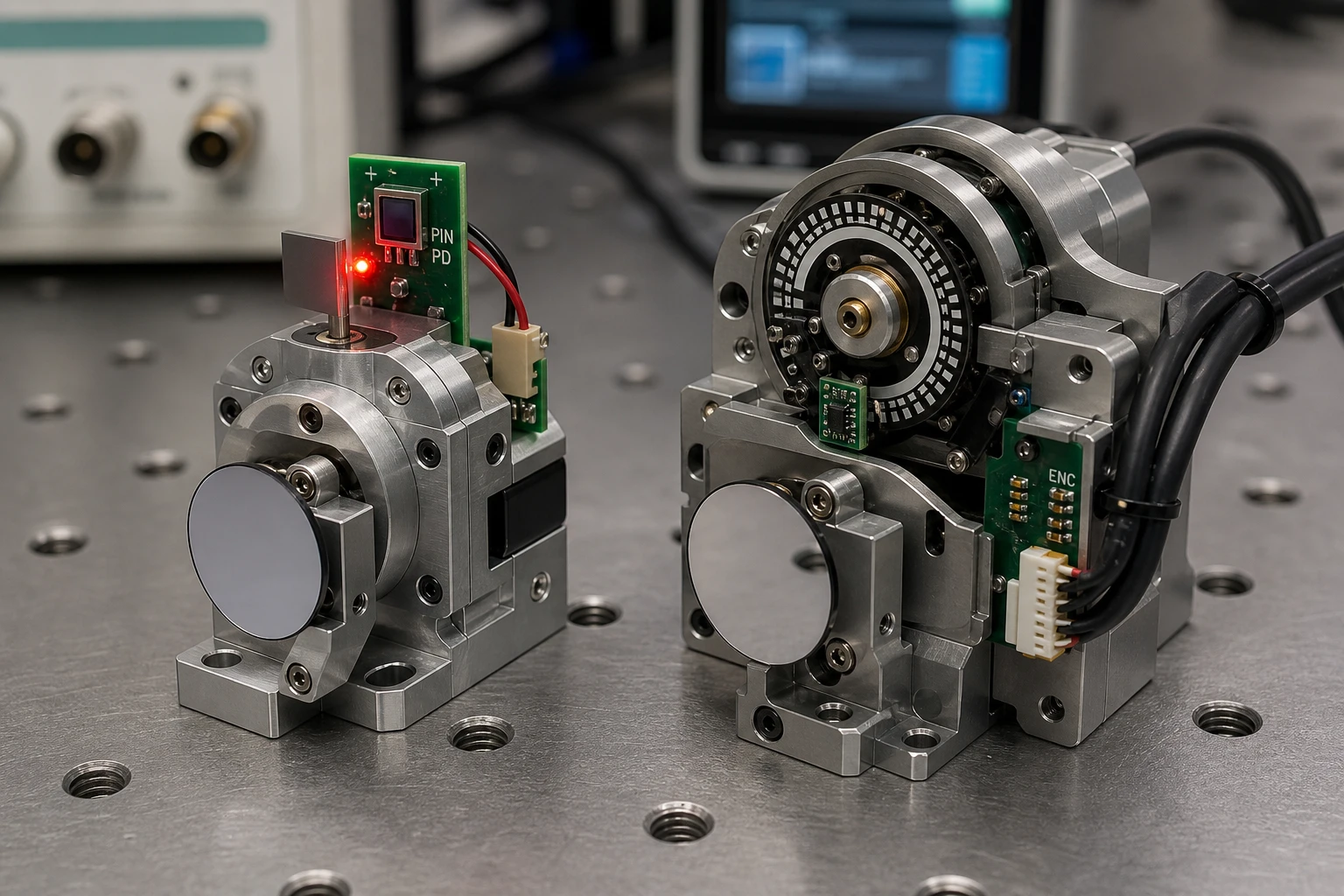
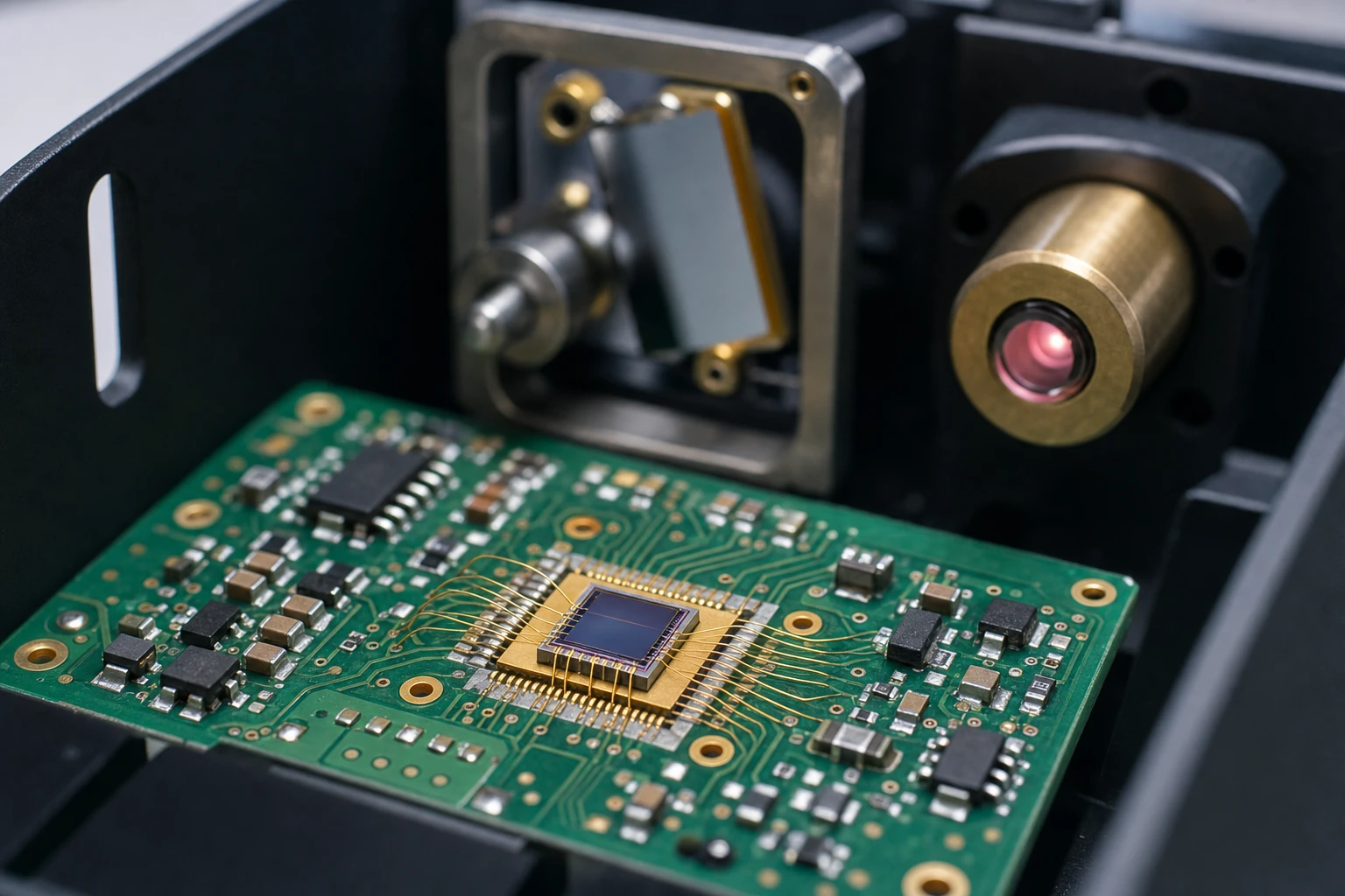
If you have ever spent weeks chasing micro-radian position drift in a high-speed galvanometer scanner, you know the frustration. You tune your PID control loops, shield your transimpedance amplifiers, pick 0.1% precision resistors, and isolate your thermal sources. Yet, as soon as the optical scanning head runs for twenty minutes, the zero-position wanders. Or worse, small laser power dips register as physical mirror movements, tricking your servo loop into driving correcting currents that shouldn’t be there.
In high-end optical scanning head design—whether for sub-micron laser micro-machining, semiconductor wafer inspection, or high-speed additive manufacturing—position feedback accuracy is everything. Traditional single-element position sensors or off-the-shelf light meters just don’t cut it anymore. High-performance scanner heads demand differential feedback systems built around a specialized segmented PIN photodiode chip.
In this article, we’ll break down the underlying optical physics, examine why single-element optical detectors fall short, dive into the mechanics of dual-channel differential rejection, and explore how selecting the right segmented PIN photodiode chip can transform your galvo feedback architecture from a noisy headache into a rock-solid, sub-microradian positioning system.
The Core Problem with Single-Element Feedback in Laser Galvos
To understand why a segmented PIN photodiode chip is essential, let’s first look at what goes wrong inside a standard galvanometer feedback loop when using basic optical sensing.
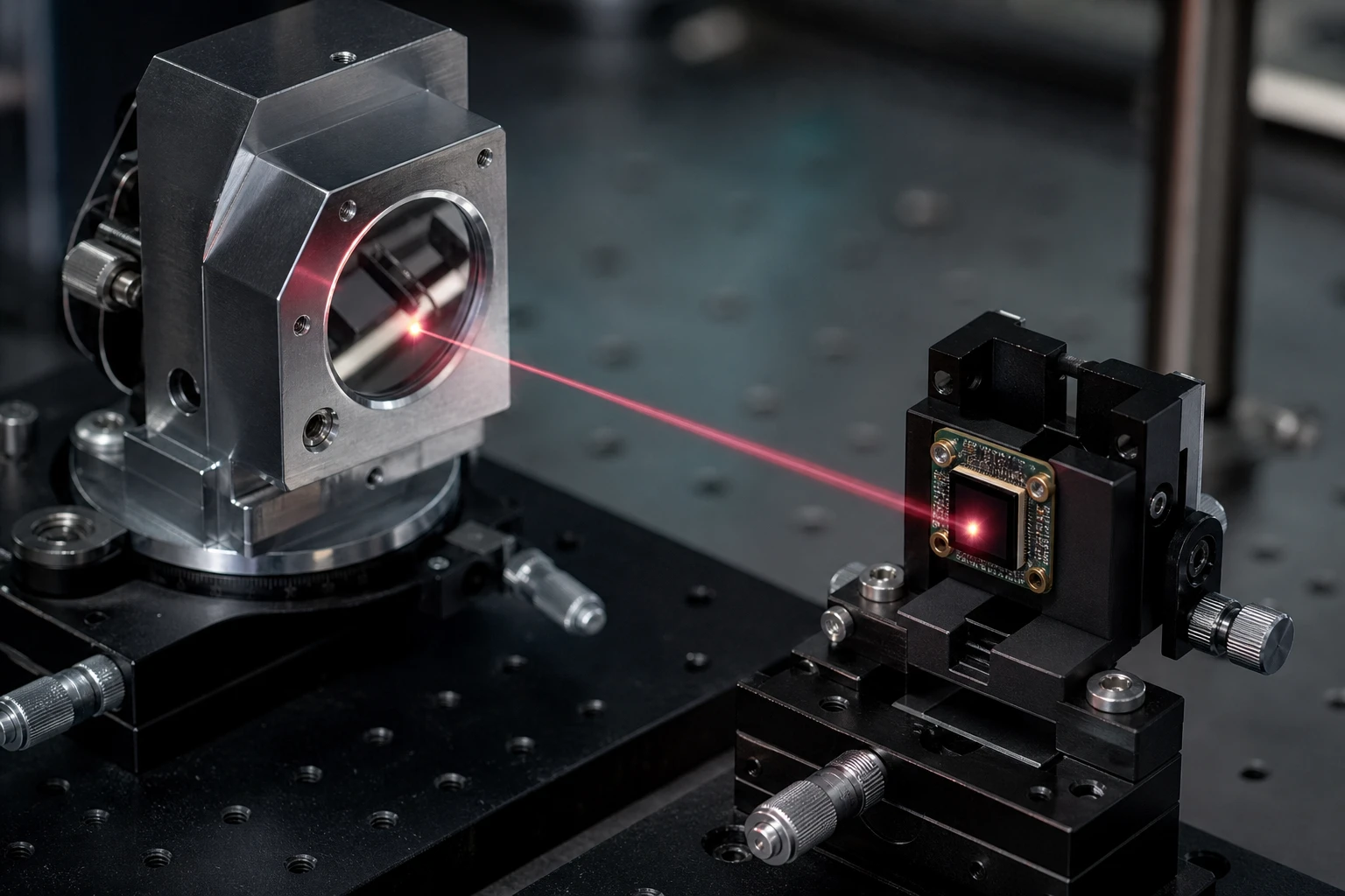
In a conventional galvo, a light source (usually an LED or an infrared VCSEL) reflects off a small moving aperture or standard optical target attached to the rotating galvo shaft. This reflected light hits a photodetector. The amount of light striking the detector is supposed to correspond linearly to the angular position of the mirror shaft.
It sounds simple on paper. But in real-world industrial environments, this single-ended measurement approach breaks down quickly due to three major non-positional noise variables:
1. Optical Source Intensity Fluctuation
LEDs and laser diodes don’t emit a perfectly constant photon stream over time. Power output varies due to drive current ripple, thermal heating of the junction, and basic semiconductor aging. In a single-detector setup, if your feedback LED drops in intensity by 1%, your optical encoder registers that drop as a physical mirror movement. The servo controller responds instantly by turning the mirror, creating a position error out of nowhere.
2. Thermal Drift and Substrate Expansion
As the galvo motor drives back and forth at hundreds of Hertz, the internal housing temperature rises. A standard silicon photodiode has a temperature coefficient that alters its responsivity (A/W) as temperature shifts. If the ambient temperature inside the scan head rises by 15°C, single-element responsivity shifts enough to throw off calibrated scan boundaries.
3. Stray Radiation and System Noise
High-power processing lasers generate diffuse back-reflection. Combine that with switching noise from nearby motor drive electronics, and a single photodiode channel absorbs all this noise directly into its feedback signal without any native mechanism to subtract it out.
When you are aiming for positioning repeatability under 5 micro-radians, intensity-based single-channel sensing fails completely. To eliminate these non-positional errors, optical engineers turn to differential spatial detection using a dual segment photodiode.
How Differential Feedback Works: The Physics and Math
Instead of measuring the absolute light power coming off the galvo optical target, differential optical position sensing measures the spatial balance of light split across two distinct, closely spaced detector elements.
When a moving light beam or shadow edge falls across a 2 segment silicon detector, the total light power P_total is distributed between Segment A and Segment B as P_A and P_B.
The individual photocurrents generated by each segment are:
- I_A = R_A * P_A + I_darkA
- I_B = R_B * P_B + I_darkB
Where R_A and R_B represent the spectral responsivity (in Amperes per Watt) of each silicon segment, and I_dark is the internal reverse dark current.
The Ratio Metric: Common-Mode Rejection
Instead of using I_A or I_B directly, the feedback circuit processes the normalized differential output signal, often called the Normalized Position Signal (NPS):
- NPS = (I_A – I_B) / (I_A + I_B)
Look closely at what happens when the light source intensity fluctuates by a scaling factor k (so P_A becomes k * P_A, and P_B becomes k * P_B):
- NPS_new = (k * I_A – k * I_B) / (k * I_A + k * I_B)
- NPS_new = k * (I_A – I_B) / (k * (I_A + I_B))
- NPS_new = (I_A – I_B) / (I_A + I_B)
The intensity scaling factor k cancels out completely!
This mathematical relationship provides Common-Mode Rejection (CMR). Any disturbance that affects both photodiode segments equally—such as LED power decay, uniform thermal expansion, or global power supply voltage ripple—is treated as common-mode noise and effectively erased from the position feedback signal.
To achieve this level of cancellation in real life, however, the two photodiode segments cannot be two separate discrete photodiodes glued next to each other. They must be manufactured together on a single monolithic silicon wafer as a true segmented PIN photodiode chip.
Spatial Ray-Trace Architecture:
- Incident Light Spot: A moving optical beam bridges across both Segment A and Segment B simultaneously.
- Monolithic Substrate Isolation: Both segments share the same temperature gradient, ensuring identical responsivity shifts across thermal cycles.
- Signal Output Processing: The analog front-end computes Position = (I_A – I_B) / (I_A + I_B), stripping out optical amplitude fluctuations instantly.
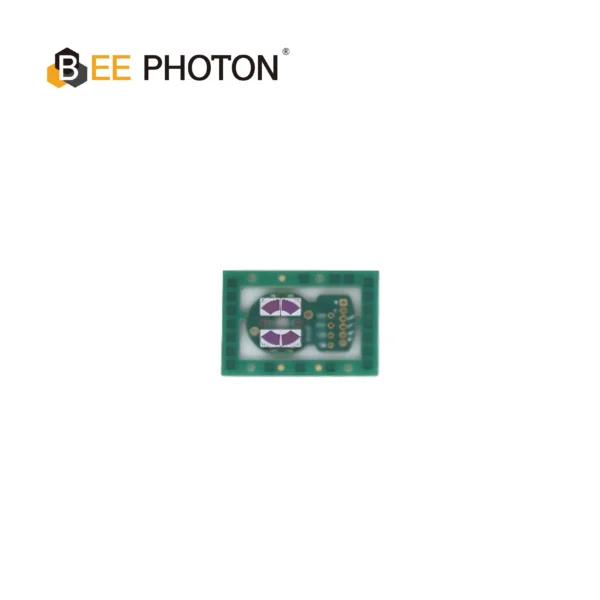
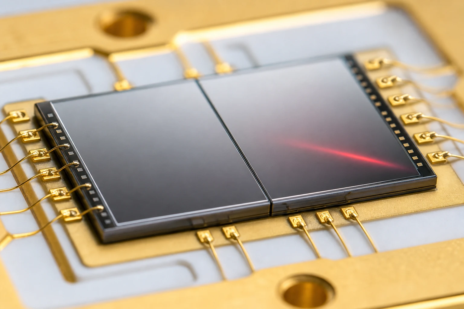
Si PIN photodiodes for Galvo PDC-2C3432-NIR-B
The PDC-2C3432-NIR-B is a specialized segmented PIN photodiode chip engineered for precise differential position feedback in high-speed galvanometer scanners. Integrating this dual-channel segmented PIN photodiode chip allows systems to obtain accurate angular tracking with minimal signal noise.
Essential Architectural Features of a High-Performance Segmented PIN Photodiode Chip
Not all dual-segment sensors are built equal. If you drop a cheap, wide-gap dual photodiode into a galvanometer encoder, you’ll run into serious non-linearity issues near the central tracking zero-point. Designing an ultra-precise differential feedback photodiode requires specific semiconductor architecture features:
1. Ultra-Narrow Inter-Segment Gap Width
The physical separation (gap) between Segment A and Segment B creates an optical “dead zone.” If the gap is too wide (e.g., >50 microns), light falling into the gap generates carrier pairs that recombine without contributing efficiently to either terminal current. This produces a flat spot or non-linear kink right at the zero-differential position—the exact point where your galvo needs maximum sensitivity.
Modern specialized chips, like the Si PIN photodiodes for Galvo PDC-2C3432-NIR-B, feature gap widths optimized down to 10–15 microns. This narrow separation minimizes transition dead zones, ensuring sub-micron positional linearity as the light spot crosses from segment to segment.
2. High Responsivity Matching and Uniform Substrate Doping
For common-mode rejection to exceed 40 dB, the responsivity matching between Segment A and Segment B must be nearly perfect:
- Responsivity Mismatch (%) = (|R_A – R_B| / R_average) * 100
If R_A and R_B differ by even 1%, light intensity changes won’t cancel out completely in the (I_A – I_B) numerator. Monolithic fabrication on high-resistivity silicon wafers allows manufacturers like BeePhoton to achieve responsivity matching tight enough (<0.15% variation) to deliver ultra-stable differential signals across broad operating temperature ranges.
3. Low Junction Capacitance for High Bandwidth
High-speed optical galvos need feedback control loops running at sampling rates well above 100 kHz, with sensor bandwidths reaching into the tens of Megahertz. The junction capacitance (C_j) of each segment acts as a low-pass filter when paired with the feedback resistor in a Transimpedance Amplifier (TIA).
By utilizing a PIN structure—inserting an intrinsic (I) high-resistivity layer between the p-type and n-type silicon—the depletion layer width increases dramatically under reverse bias. This lowers junction capacitance to around 10–15 pF per segment at -5V bias, allowing rapid signal response times (<10 ns rise time) without inducing phase lag or ringing in the servo loop.
4. Crosstalk Isolation
Optical and electrical crosstalk between adjacent segments can ruin differential independence. If carriers generated under Segment A diffuse laterally into Segment B’s depletion region, signal isolation degrades. Modern segmented PIN photodiode chip designs incorporate localized isolation channels or guard rings embedded between segments to keep inter-channel crosstalk lower than -40 dB.
Comparing Feedback Architectures: Single-Element vs. Dual Segment PIN Photodiodes
When choosing components for high-end galvo position detectors, comparing engineering metrics directly highlights why dual-segment differential architecture is the industry standard for high-precision design.
| Parameter / Metric | Standard Single-Element PIN Photodiode | Monolithic Dual Segment PIN Photodiode Chip | Impact on Scanner Performance |
|---|---|---|---|
| Primary Sensing Method | Absolute Intensity (Power) | Differential Spatial Ratio (I_A – I_B)/(I_A + I_B) | Rejects illumination source noise and drift |
| Common-Mode Noise Rejection | 0 dB (None) | > 45 dB | Prevents laser power variations from registering as mirror tilt |
| Thermal Drift Sensitivity | High (~0.2% / °C responsivity drift) | Ultra-Low (<0.01% / °C differential offset drift) | Eliminates zero-point drift during long operational cycles |
| Position Linearity Range | Poor (dependent on beam power profile) | Highly Linear across narrow segment boundary | Enables precise micro-stepping and sub-microradian repeatability |
| Junction Capacitance (per channel) | Varies (~50-200 pF for large active areas) | Low (<15 pF at -5V reverse bias) | Higher bandwidth, enabling faster servo update loops |
| System Calibration Complexity | Requires frequent recalibration | Factory baseline stable over long durations | Lowers long-term maintenance costs for end-users |
Real-World Case Study: Resolving Drift in a Micro-Machining Scan Head
To see how this works in practice, consider a real engineering scenario involving an industrial laser micromachining system used for drilling micro-vias in flexible PCBs.
The Challenge
A manufacturer was using a single-element optical encoder setup inside their galvanometric scan head. While initial positioning accuracy immediately after dynamic calibration met specs, performance degraded after 30 minutes of continuous high-speed raster scanning.
- Observed Problem: Zero-position drift exceeded 25 micro-radians after thermal stabilization.
- Root Cause Analysis: The feedback LED temperature rose from 25°C to 48°C during operation. This thermal rise caused a 3.2% drop in LED light output. The single-element position detector interpreted this power loss as mirror rotation, causing the servo motor to drift off-target to compensate for error that didn’t physically exist.
The Solution
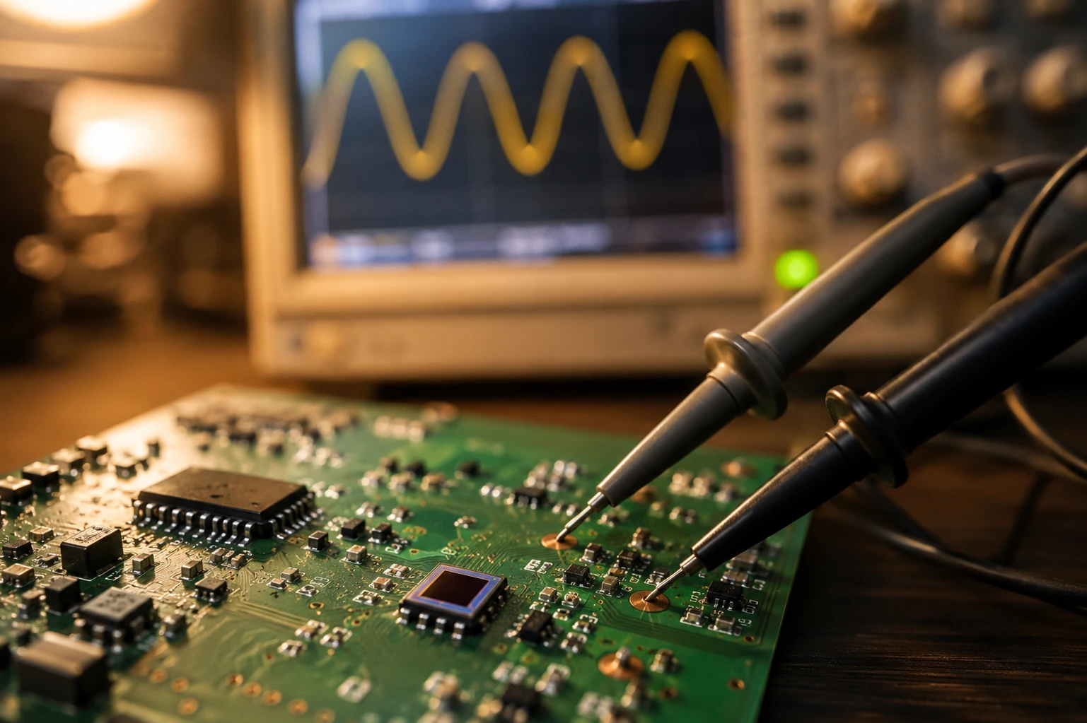
The engineering team redesigned the optical position pickup to use a differential optical geometry built around the Si PIN photodiodes for Galvo PDC-2C3432-NIR-B. This 2 segment silicon detector was paired with a dual-channel transimpedance amplifier feeding a normalized differential processing circuit.
Architecture Comparison Overview:
- Traditional Single-Element Pickup: LED Source -> Galvo Target -> Single Photodiode -> Servo Error! (LED power drops 3.2% -> System misinterprets as a 25 µrad position shift).
- Upgraded Differential Pickup: LED Source -> Galvo Target -> Segment A / Segment B -> Normalized Ratio (A-B)/(A+B) -> Stable Position Signal (LED power drops 3.2% -> Both channels drop equally -> Ratio remains perfectly constant!).
The Results
- Position Drift Reduction: Zero-position drift dropped from 25 micro-radians to under 1.8 micro-radians over a 4-hour continuous burn-in run.
- Noise Immunity: Intentional 10% supply voltage ripple applied to the feedback LED driver resulted in zero measurable mirror jitter on the laser target.
- Dynamic Bandwidth: Thanks to the low capacitance of the segmented PIN photodiode chip, feedback bandwidth easily exceeded 35 MHz, allowing the galvo step-and-settle time for a 1-degree step to drop from 220 microseconds to under 140 microseconds.
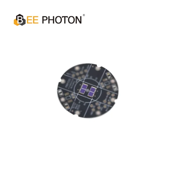
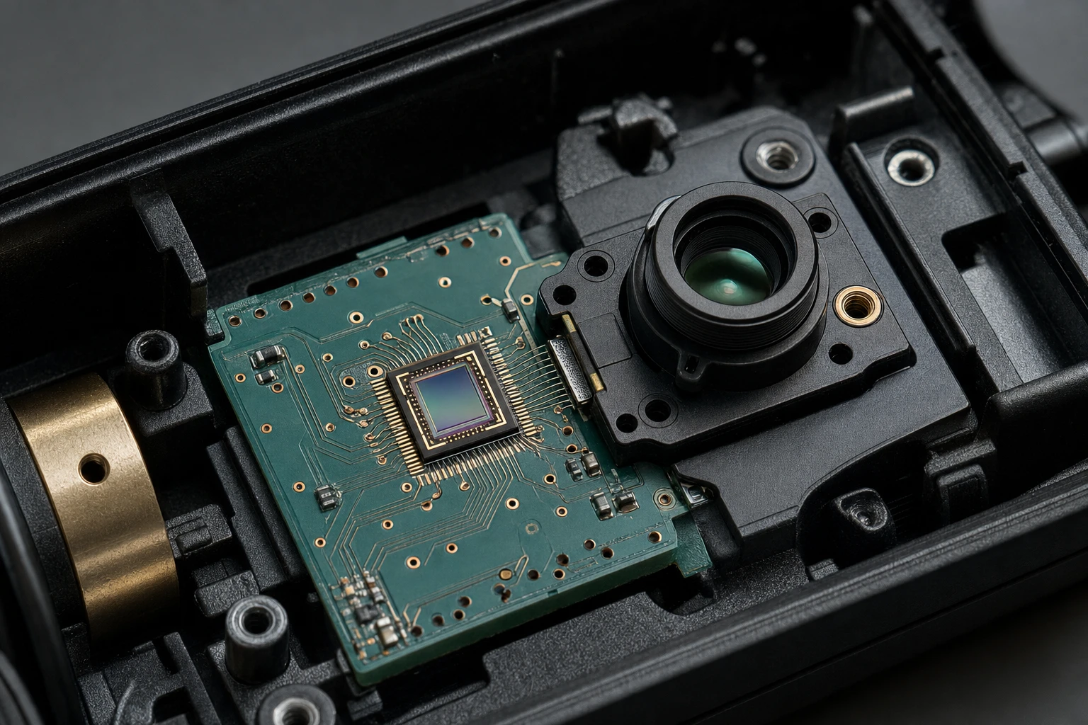
Si PIN photodiodes for Galvo PDC-C2928-NIR-B
Optimize scanning with our 940nm PIN photodiode chip, PDC-C2928-NIR-B. This 940nm PIN photodiode chip ensures precise galvo position sensing and low noise.
Selecting the Right Silicon Architecture for NIR Galvo Feedback
When picking a chip for your galvo position encoder, matching the detector’s spectral responsivity peak to your optical feedback source wavelength (usually Near-Infrared, 850 nm – 950 nm) is vital to maximize signal-to-noise ratio.
Depending on your optics and target layout, different photodiode choices offer distinct trade-offs:
1. Dual-Segment Differential PIN Chips
For high-speed differential position decoding, monolithic dual-segment chips are the preferred solution. Options like the Si PIN photodiodes for Galvo PDC-2C3432-NIR-B offer specialized NIR-enhanced silicon engineered for high responsivity at 940 nm (~0.60 A/W), tight segment matching, and minimal gap dead-space.
2. Single-Element NIR Reference Detectors
If your scanner design uses a secondary monitor channel to measure absolute beam intensity independently, pairing differential sensors with dedicated single-element NIR chips works well. High-responsivity options like the Si PIN photodiodes for Galvo PDC-C2928-NIR-B (optimized for 940nm LED/VCSEL light sources) or the Si PIN photodiodes for Galvo PDC-C2929 (tuned for 920nm emission peaks) provide fast response times and clean baseline signals for calibration loops.
Technical Design Considerations for Board Layout
When dropping a differential feedback photodiode onto your PCB design, keep these practical layout guidelines in mind:
- Symmetric Trace Routing: Route traces from Segment A and Segment B to your TIA amplifier inputs symmetrically. Unequal trace lengths add parasitic capacitance differences that degrade high-frequency common-mode rejection.
- Guard Ring Grounding: Surround the high-impedance photodiode node traces with ground guard rings to prevent surface leakage currents from distorting the micro-ampere level photocurrents.
- Reverse Bias Voltage Stability: Drive the common cathode (or anode, depending on polarity) with a low-noise, well-filtered reverse bias supply. While differential processing cancels out common power supply fluctuations, high frequency bias noise can degrade the depletion region uniform width across both segments.
Technical Comparison Matrix: Segmented PIN Options for Optical Galvos
To help select the proper detector structure for your galvo sensing project, here is a breakdown of how key specifications impact feedback performance:
| Feature Requirement | Recommended Detector Type | Key Engineering Advantage |
|---|---|---|
| Sub-Microradian Angular Feedback | Dual Segment PIN Chip (e.g., PDC-2C3432-NIR-B) | Cancels thermal and LED intensity noise via ratio processing. |
| Direct Intensity Monitoring | Single-Element NIR PIN (e.g., PDC-C2928-NIR-B) | Broad active area, high speed, optimized for 940nm emitters. |
| Custom Sub-Assembly / Hybrid Module | Bare Chip Die on Ceramic/Substrate | Minimizes stray capacitance and geometric footprint inside galvo. |
Frequently Asked Questions (FAQ)
Q1: Why can’t I just use two separate single-element photodiodes mounted side-by-side instead of a segmented PIN photodiode chip?
While using two separate photodiodes seems like a quick workaround, it rarely performs well in high-precision differential scanning. Discrete photodiodes come from different areas of a silicon wafer (or even different wafer batches), meaning their responsivity temperature coefficients (ppm/°C) and dark current curves won’t match tightly. Additionally, the physical gap between two separate packaged diodes is usually several hundred microns wide—far too large for micro-radian galvo position feedback. A monolithic segmented PIN photodiode chip ensures identical thermal performance, identical silicon doping, and gap widths down to 10–15 microns.
Q2: What is the ideal light spot size relative to the gap width on a 2 segment silicon detector?
For linear differential response, the focused light spot striking the detector must be significantly larger than the inter-segment gap width, but smaller than the total active area of both segments combined. As a rule of thumb, a spot diameter roughly 2x to 5x the gap width provides a smooth, highly linear transfer function near the central null point. If the beam spot is too small (approaching the gap width), small movements within the gap won’t produce measurable photocurrent shifts, creating a dead band in your servo control loop.
Q3: How does reverse bias voltage affect the performance of a differential photodiode in galvo applications?
Applying a reverse bias (typically -3V to -10V) expands the intrinsic depletion layer inside the PIN junction. This reduces capacitance per segment, speeding up response times and enabling higher feedback bandwidth. It also lowers carrier transit time across the junction, reducing phase lag in your servo feedback loop. However, higher reverse bias increases dark leakage current slightly, so choosing an optimized chip with ultra-low dark current specs (<0.5 nA at -5V) is key to keeping thermal noise low.
Q4: Can a dual segment photodiode compensate for physical mechanical tilt in the scanner housing?
Differential signal processing cancels out optical intensity fluctuations, power supply noise, and uniform thermal drift across the detector active area. However, it cannot distinguish between mirror rotation and physical mechanical deformation (such as housing warp) that shifts the optical baseline path. Good mechanical thermal isolation remains necessary, but switching to a dual segment photodiode removes the primary source of drift: optical power and emitter temperature instability.
Ready to Upgrade Your Optical Feedback Loop?
Building next-generation laser galvo scanners requires component choices that match your precision targets. If micro-radian drift, low signal bandwidth, or thermal instability are holding back your scanner design, upgrading your position pickup to high-reliability differential silicon sensing is the single most effective hardware step you can take.
At BeePhoton, we specialize in high-performance silicon PIN photodiode chips designed specifically for demanding optical position detection, industrial galvo control, and photonics applications.
Whether you need high-uniformity dual-segment chips like the Si PIN photodiodes for Galvo PDC-2C3432-NIR-B, or optimized single-element monitor diodes such as the PDC-C2928-NIR-B and PDC-C2929, our engineering team can help you select, customize, and integrate the right photodetector silicon into your optical architecture.
Take the Next Step:
- Explore Product Specifications: Visit BeePhoton to browse our full lineup of photodiode chips, custom die options, and technical datasheets.
- Request Custom Samples or Technical Guidance: Have specific requirements for gap geometry, die size, or customized spectral responsivity matching?
- Get in Touch Directly: Email our application engineering team at info@photo-detector.com or submit an inquiry through our direct contact BeePhoton technical team form.